

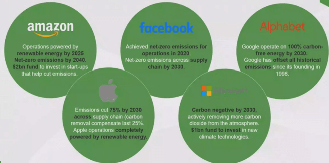
During the recent Applied Materials/SEMI Sustainability Forum, panelists touched on the fact that the big drivers of electronics — Apple, Amazon, Alphabet, Microsoft, and Facebook — are looking to cut carbon emissions across their supply chains.
From a semiconductor perspective, this would include the energy and greenhouse gases used in the manufacturing of the chips, which then trickles down to the equipment suppliers and the material manufacturers. This will be a somewhat challenging task for the industry, as many of the chemistries and the basics of the processes such as cleaning wafers, dry etching, and deposition techniques have been around without changes since the early days of the industry.
How do We Achieve Semiconductor Sustainability?
Changes to processes and equipment tend to happen when a new node or technology is introduced. Changes such as extreme ultraviolet (EUV) lithography uses different resists than deep ultraviolet (DUV) lithography technology. 3DNAND introduced new etch and deposition processes. DRAM capacitor processes and materials have been evolving as greater storage capacitance is needed.
Changes can also happen when significant improvements in yield or lower costs can be achieved by changing the process. However, this tends to be the exception rather than the rule. In making changes to reduce our carbon footprint, there is also the challenge of legacy nodes, which now are getting a lot of press because of the semiconductor shortage. These chips are built on 4-, 6- and 8-inch wafers, with processes that were developed to achieve a high yield at the lowest costs. Most likely the process recipes haven’t been changed since the fab started producing that chip in volume. And one challenge I haven’t heard mentioned at the semiconductor sustainability events I have attended is that if a process is changed, the chip needs to go through a re-qualification process to ensure it will perform identically to the chips using the old process. This takes time as well as money to make that happen. In projects I’ve worked on in the past, some companies are reluctant to make changes due to the cost, time, and the fact that making these changes will cut into razor-thin margins. With these caveats, will the chip industry really be able to make progress towards lower power consumption, and a reduction in greenhouse gases?
Hopefully, there are significant changes in the mix that will help move the needle on semiconductor sustainability. In November, I wrote on CEA-Leti’s paper presented at the European Solid-State Device Research Conference (ESSDERC) and the European Solid-State Circuits Conference (ESSCIR), which outlines 9 research tracks for the semiconductor industry to lower its carbon footprint.
Will Apple Lead the Way?
In November IMEC announced that Apple has Joined IMEC’s Sustainable Semiconductor Technologies and Systems (SSTS) research program. Apple is making a strong sustainability statement in joining this alliance. At the Sustainable SEMI Venture Conference, Ajit Manocha, president, and CEO of SEMI pointed out that one of Apple’s sustainability goals was to cut emissions 75% by 2030 across their entire supply chain. For Apple, this is a big undertaking, as they do very little in-house manufacturing. From a semiconductor perspective, it also has far-reaching ramifications as Apple is both a fabless company, using TSMC for a significant number of their advanced chips, and they also use many other semiconductor manufacturers such as Siemens, for chips in their products that use older process nodes. Thus, Apple’s goals will impact a broad swath of the chip industry.
In a discussion with Lars-Ake Ragnarsson, the scientific director of the SSTS program, he said the IMEC SSTS program sets out to develop a set of concrete and reliable models, and detailed (carbon) footprint analyses, that then help the industry better determine the carbon and environmental footprint of the specific processes they are using.
According to IMEC approximately 75% of a mobile device’s carbon footprint can be attributed to fabrication with close to half of that from the underlying manufacturing process. By developing the models and the data, IMEC will help material, equipment, chip, manufacturers, and electronics device manufacturers to understand and be better able to estimate their carbon footprint. Hopefully, they can then take measures to reduce the amount of greenhouse-producing materials used, as well as reduce the amount of energy it takes to produce a chip.
Ragnarsson mentioned that IMEC currently estimates that the number of greenhouse emissions will or have increased by 3.5 times as the industry transitioned from 28nm to 3nm. While the industry today is focused on power performance and cost, (PPC) decisions will need to be made in the near future with respect to green, or environment, thus changing the PPC, or Applied Materials longer PPAC acronym to either PPCG for green or PPCE for environmental.

Reducing the semiconductor industry’s GHG emissions will likely come with added costs, and possibly longer cycle times. Innovative solutions will need to emerge to replace some of the processes that consume large amounts of energy. New materials will need to replace the ones that create high greenhouse gas emissions such as SF6 and NF3. Solutions to reduce fab energy expenses associated with the circulation of air for cleanrooms will also need to be addressed. Water usage and waste reduction will also need to be addressed to achieve a complete or at least a working solution to assist companies in meeting environmental goals.
The Industry is Off to A Good Start
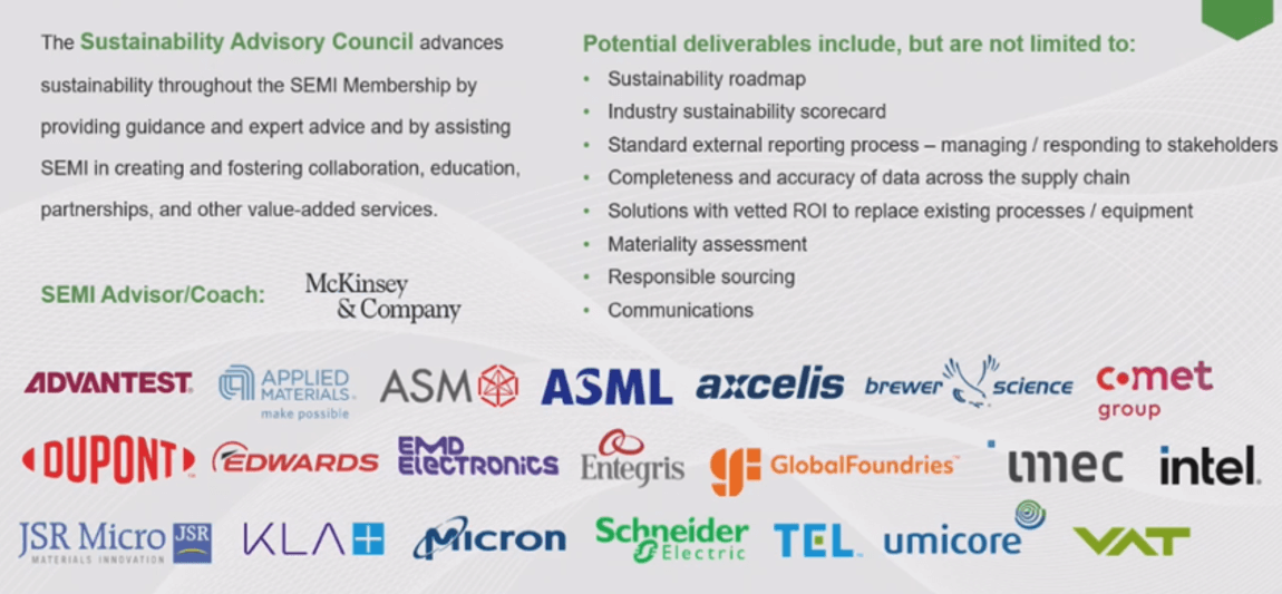
As leaders in semiconductor sustainability, Intel, ST Microelectronics, and ASE have been looking at some of these environmental issues for a considerable amount of time. But, to reach a tipping point to turn the carbon dial back, more collaboration will be needed. Both the CEA Leti, and IMEC’s programs will work with paying partners to help push the work forward, but these are separate programs, as opposed to the working partnership we heard about at IEDM a few years ago. SEMI has created an advisory council, but it’s a short list when one looks holistically at the industry, and major players or influencers are missing from the list.
In the short term, it will have to do; however, in the longer term, the industry will need to come together to ensure that the optimum GHG solutions have been implemented and that the industry is looking at reducing power and waste, versus just implementing 100% renewables and calling it a day.


