
Continuing our look at presentations from the IMAPS SiP Conference.
Ajinomoto
Habib Hichri of Ajinomoto discussed the use of novel dielectric materials for fine RDL in 5G applications. IFTLE has discussed ABF films in previous blogs [ see IFTLE 479 “ABF substrate shortages…”]. High-speed transmission and large body size require low dielectric loss and low CTE.
The process flow for substrate manufacturing using ABF film is shown in Figure 1:
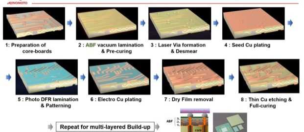
Figure 2 shows ABF grades in commercial production:
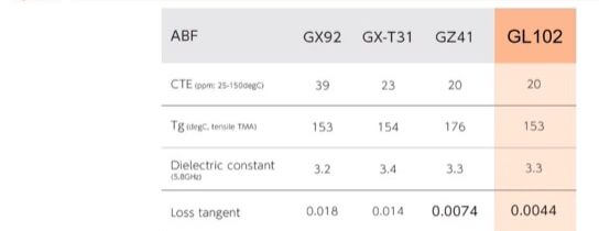
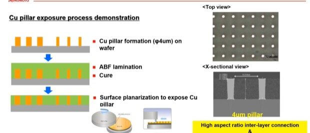
Figure 3 shows Ajinomoto’s new nanofiller ABF, which is under development for 2/2 L/S RDL and can be used in a via-less process:
Ajinomoto is also developing liquid (MI series) and film molding materials (LE series) for System in Package (SiP) and fan-out wafer-level packaging (FO-WLP). The major advantage is the low warpage property.
BESI
Chris Scanlan discussed advanced die attach for the chiplet era. Besi is a leading global supplier of advanced packaging assembly equipment including die-attach, molding, and plating equipment.
Chiplet technology will require extremely high density and thus higher placement accuracy (Figure 4).

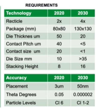
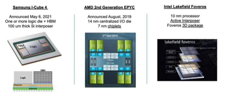
Figure 5 shows some examples of real announced chiplet products that will require a lot of placements because they all have different bonding requirements.
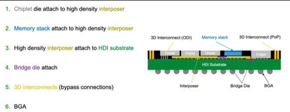
You may find all of the following in the same chiplet SiP module (Figure 6).
As pitches go below 10µm or so, the assembly will be moving to so-called “hybrid bonding” using a copper – copper bond without any solder. The first applications will be in high-performance computing. Eventually, stacked memory will likely move to hybrid bonding.
As we discussed earlier in the year ( see IFTLE 475, “EPTC 2020: IME on Hybrid Bonding…..” ) hybrid bonding has been used for almost a decade in CMOS image sensor products and has more recently been shown on the advanced packaging assembly roadmaps of Intel, Samsung, and most of the advanced packaging houses.
For all the latest in Advanced Packaging stay linked to IFTLE………………………………………….


