iMAPS: Enabling a Connected World: Always On!
3D InCites will be participating in the iMAPS 2020 virtual symposium, October 5-8, 2020. Come check out our virtual profile to learn more about our community membership and 2021 editorial and marketing opportunities. We have compiled a list of papers, presentations and exhibitor previews of our community members participating in the show. Read more for full details.
Panels, Papers and Discussions
Tuesday, Oct. 6
3:00pm-4:30pm Eastern
Feature Panel Sponsored by Amkor Tehnology
The Future Advanced Packaging Ecosystem: Who Will Be in the Driver’s Seat?
Chair and Moderator:
Jan Vardaman, TechSearch International
Panelists:
Koushik Banerjee, Intel Corp.
Dan Berger, GLOBALFOUNDRIES
Eelco Bergman, ASE
Mike Kelly, Amkor Technology
Khai Nguyen, NVIDIA
Craig Orr, Samsung
Ashkan Seyedi, HPE
As the industry moves to the next silicon nodes, new advanced semiconductor packaging developments are enabling the economic gains that were previously achieved with monolithic silicon scaling. Co-design of IC and package becomes increasingly important. The foundry plays an increasingly important role. Development of a healthy eco-system is critical to providing solutions to meet our industry needs. This panel will discuss the eco-system, challenges the industry faces, and the roles for the players.
1:30pm-2:30pm Eastern
“One Year Later – What’s Changed in 2020”
Moderator: Priya Mukundhan, Onto Innovation
A roundtable discussion hosted by the IMAPS Diversity and Inclusion Committee
Join Priya Mukundhan of Onto Innovation for a roundtable discussion with attendees and key conversationalists about how the events of 2020 have changed the diversity and inclusion landscape in the industry.
This session will be conducted via Zoom. Attendees are encouraged to participate in this discussion. No session pre-registration required!
1:00pm-3:00pm Eastern (Tuesday and Thursday)
Professional Development Courses
Course A8:
The Evolution of Flip Chip Package Technology
Mark Gerber, ASE US, Inc.
This PDC course will provide a historical overview and background on the evolution of flip chip packaging as well as short market perspective on this platform. Mobile, Infrastructure, Automotive, High Reliability, Medical and High-Performance Network and Computing all rely on Flip Chip technology to enable their silicon solutions. Although the use of new technologies such as Fan-Out hold promise for certain applications, flip chip advancements continue to challenge many new technology competitors from a price and reliability perspective and may end up driving hybrid approaches. Interconnect structure, process flows, materials and package integration process methods for evolving Flip Chip applications will be discussed in detail. Understanding the trade-offs between the different bump structures and package platforms is key in determining the silicon device layout and the type of design rules that can be leveraged for new products. As part of this course, the assembly process details will be discussed and will include Mass Reflow, Thermo-Compression Non-Conductive Paste (TCNCP) bonding and Laser Assisted Bonding. Reliability aspects such as IMC formations and ways to address will also be covered as a key consideration for Interconnect decisions.
Wednesday, Oct. 7
3:00pm-4:oopm Eastern
IMAPS Student-Industry Roundtable Discussion
An industry panel followed by a Q&A session for students breaking into the industry.
Join moderator Erica Folk of Northrop Grumman for an interactive discussion between industry leaders and students focused on taking the next steps into your professional career. Hear from early, mid-, and senior-level microelectronics industry professionals about what they’re looking for in new hires, how to succeed in the modern workforce, and what to expect as you progress to the next level. Come with questions and begin your networking journey!

Moderator: Erica Folk, Northrop Grumman
Panelists/Q&A Team:
Beth Keser, Intel
Mark Gerber, ASE Group
Mary Pickens, Novelis
Nicole Wongk, Honeywell
Jenny Shen, Facebook
Dan Krueger, Honeywell
Exhibitor Previews
StratEdge Corporation
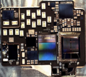
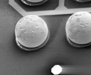
Optimizing High Power GaN Device Performance With Eutectic Die Attach
 StratEdge Corporation, founded in 1992, designs and manufactures high-performance semiconductor packages operating from DC to 63+ GHz as well as provides chip assembly and test services. The company has a complete line of post-fired ceramic and MIL-STD hermetic molded ceramic and ceramic QFN semiconductor packages.
At iMAPS, learn about its new line of packages for the extreme demands of GaN devices and the eutectic die attach process that produces extremely thin, low-void bond lines between the device and package heat sink. StratEdge also provide the same service for die-on-tab. To make an appointment to hear more about the 6 micron thick, AuSn die attach process that produces >96% coverage visit www.stratedge.com/imaps.
Finetech
Providing an Equipment Pathway for R&D/Prototyping to Production
Learn more about Finetech’s high‐accuracy bonding equipment in support of today’s most precise and complex applications. Its portfolio of bonders provides an equipment pathway from prototype to automated production, with a unique capability to run the automated models in manual mode for true flexibility.
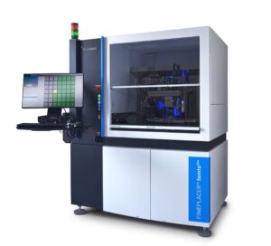
New to the FINEPLACER® family, the FINEPLACER® femtoblu bonding system, is an automated micro assembly cell providing an efficient and economical solution for dedicated photonic production. These demanding applications will benefit from a placement accuracy of 2.0 µm @ 3 Sigma and ultra-low force bonding capability down to 5 gram-force. Designed for prototyping and high-yield production duties, the system supports all bonding technologies specifically required for the assembly of photonic and optoelectronic components. Visit https://www.finetech.de/welcomeimaps/ for more information.
JIACO Instruments
Decapsulation Technology Solutions
Discuss potential decapsulation solutions and get a preview of its machine at the virtual Jiaco booth. Learn how the company can assist with your challenging decapsulation requirements for reliability test, quality control and failure analysis or how to decapsulate 2.5D, Ag wire, Cu wire, 3D IC, SiP, WLCSP, GaN, GaAs, automotive package, fresh and thermally stressed devices etc. with its novel atmospheric pressure artifact-free decapsulation technology.
Contact info@jiaco-instruments.com to know more or to schedule a time to speak before, during or after iMAPS.