

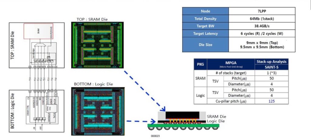
Samsung Foundry SAINT-S
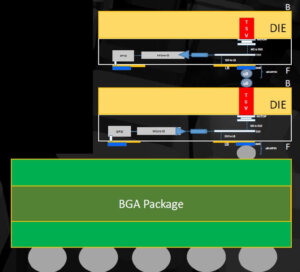
Samsung Foundry revealed their SAINT-S technology for SRAM on logic 3DIC, at the recent IMAPS Device Packaging Conference, and it is certainly worthy of a closer look. As shown in Figure 1, it is an SRAM on Logic 3DIC with 4µm TSV on 50µm pitch. It consists of face to back stacking of two 7 LPPP dies on an advanced ball-grid array (BGA) substrate.
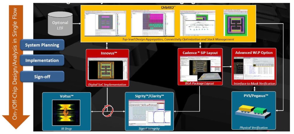
Its design (Figure 2) is accomplished using:
- Cadence OrbitIO for top-level design planning
- Cadence Innovus for die layout
- Cadence SiP Layout for BGA package layout
- Sigrity/Clarity for electrical analysis
The overall design flow is shown in Figure 3:
Note this SRAM on logic 3DIC is from Samsung Foundry so it should be available on the open market to any and all customers (with the standard OSAT proviso that you must be big enough for them to want to pay attention to your request)
KNS Formic Acid Reduction Technology
Also at the IMAPS DPC, Kulicke & Soffa presented an informative discussion on fluxless bonding via in-situ oxide reduction. Although the use of formic acid vapor for the reduction of oxides has been reported for more than a decade this is the first time anyone has taken a complete look at the chemistry behind this.
Fluxing adds thermal compression bonding complexity:
- pre-bond flux step
- post bond clean up
- underfill will not adhere to flux residues
- flux fumes clog bond heads
For large die with fine pitch oxide reduction with formic acid, vapor appears to be the answer. The chemistry is detailed in the equations below.
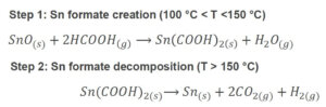
The decomposition rate of tin formate above 200°C is in the order of seconds. The schematic of the KNS delivery system is shown in Figure 4.

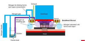
There is a shroud built into the system that keeps the formic acid vapor from migrating into the rest of the system.
KNS also sees this technology as being the bridge that leads us into direct Cu-Cu bonding.
Direct thermocompression bonding allows for sub 10µm interconnect pitch and exhibits superior electrical and thermal properties vs solder. BUT 10µm pitch copper pillar bonding is difficult due to solder extrusion and bridging. Formic acid reduction of copper oxides allows for pure metal contact.
They envision memory stacking for high bandwidth memory (HBM) being done with direct Cu-Cu bonding.
They are currently working with the UCLA CHIPS program to prove out this technology for Cu.
For all the latest in Advanced Packaging stay linked to IFTLE……………….


