
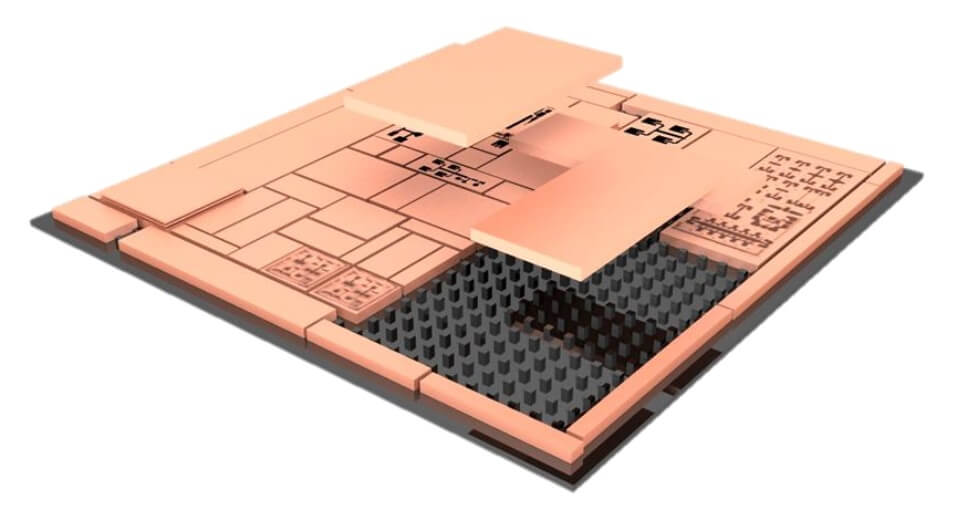
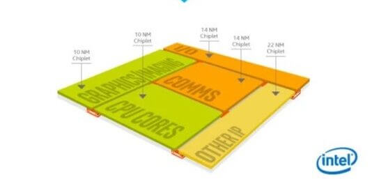
 Everyone by now should know that Intel has been a lead member of the DARPA “CHIPS” program fostering and developing standardization for the use of chiplets in which silicon IP can be developed, standardized, and easily integrated with other chiplets into a single device to deliver new levels of functionality and optimization (Figure 1). With Andreas Olofsson leaving DARPA at the end of January, that program will now be run by Gordon Keeler making him the 3rd program manager in the life of the project.
Thus, for many of you, the recent headline that “Intel joins CHIPS Alliance” may have been confusing.
The CHIPS Alliance (not to be confused with DARPA’s CHIPS program, is an organization that develops and hosts open-source hardware code (IP cores), interconnect IP (physical and logical protocols), and open-source software development tools for design and verification use in mobile, computing, consumer electronics, and Internet of Things (IoT) applications. The main aim is to provide a barrier-free collaborative environment, to lower the cost of developing IP and tools for hardware development.
As such, Intel’s goal in joining the alliance is to share their Advanced Interface Bus (AIB) protocol as an open-source, royalty-free standard for connecting multiple semiconductor die within the same package. AIB is a die-to-die PHY level standard that enables a modular approach to system design with a library of chiplet intellectual property (IP) blocks. AIB uses a clock forwarded parallel data transfer mechanism similar to DDR DRAM interfaces.
This effort within the CHIPS Alliance is intended to encourage broader adoption and support for AIB-enabled chiplets. Intel hopes to encourage the growth of an industry ecosystem for chiplet technology using its AIB protocol. AIB will be further developed in the Interconnects workgroup. AIB technical details are being placed in the CHIPS Alliance “github”.
IEEE 1838 Allows Test Access to Every Die in 3D IC Stack
For years IFTLE has preached that in order for #3DIC to become a standard industrial technology testing of the stacks had to become a standardized procedure. We are happy to report that the IEEE 1838 3D-DfT (design-for-test) standard, initiated by IMEC, allows IC vendors to design dies which, enable access to every layer in the stack, making testing using automatic test equipment much easier, has finally been fully approved.
In 2010, the IEEE 3D-Test Study Group was asked to investigate whether or not there was a need and industrial support for test and/or design-for-test standards for TSV-based 3D ICs. The IEEE working group to standardize 3D-DfT was founded in 2011 by IMECs Erik Jan Marinissen, who served as its first chair.
The aim of IEEE Std P1838 is to define, at die-level, standardized 3D-DfT features, so that when dies are stacked, a 3D-DfT test access architecture emerges in which dies and interconnect layers between adjacent stacked dies can be tested individually.

IEEE Std P1838 consists of three main components; (1) a serial control mechanism (SCM), (2) a die wrapper register (DWR) and (3) a flexible parallel port (FPP). The architecture supports:
- Pre-bond tests prior to stacking,
- Mid-bond tests on incomplete, partial stacks,
- Post-bond tests on complete yet still not packaged stacks,
- Final tests on the final packaged product.
Pre bond test access is provided either through direct probing of the fine pitch micro bumps or through optional extra probe pads on the die. The additional silicon area cost of the 3D DfT is reportedly limited and becomes negligible for standard-sized SoCs.
A schematic overview of the 3D-DfT architecture, based in IEEE 1500 based die wrappers, is shown in Figure 2.
Further details on this technology can be obtained in Marinissen’s chapter “3D Design for Test Architecture” chapter 12 in Vol 4 of Wiley-VCH Handbook of 3D Integration, Franzon, Marinissen, and Bakir Eds.
For all the latest in Advanced Packaging stay linked to IFTLE…………………………


