
 Severine Cheramy, Director 3D Business Development, at CEA-Leti, recently brought key partners of Leti’s 3D-IC programs together at the 6th 3D VLSI Open Workshop to give an overview of their accomplishments and to demonstrate synergies between their joint efforts. The event took place in mid-October at The DoubleTree Hotel in San Jose.
Leti and ST Microelectronics: Leaders in 3D VLSI
Cheramy welcomed the attendees and partner representatives to the 3D VLSI Open Workshop and highlighted the key benefits of 3D integration: Power savings, bandwidth, performance and capacity increase, cost-effective heterogeneous integration, footprint savings as well as modularity that simplifies IP reuse and customization. She provided an overview of Leti’s 3D-centric development efforts, in cooperation with several development partners, who presented later in this workshop.
According to Cheramy, Leti can now achieve 1µm pitches in wafer-to-wafer and die-to-wafer stacking using hybrid bonding technology. They are also developing ultra-fine pitch 500 nm hybrid bonding technology. In a brief update on Leti’s CoolCubeTM program, she reported that they have proved with a test chip that a 500°C thermal budget for the top layers is acceptable. She also said that Leti starts a multi-project wafer for this monolithic 3D IC solution.
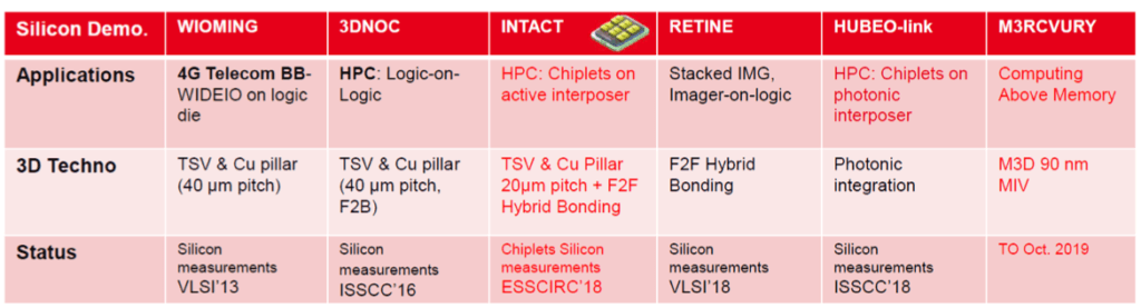
Sebastien Thuries, Design Scientist at CEA-Leti presented next. He talked about Leti’s many interposer-based and vertical stacking programs. Their names and key parameters are highlighted in Figure 1.
Thuries said the era of active (a.k.a. smart) interposers has begun (e.g. placing the I/O circuitry on the interposer) and showed examples of how interposers can simplify heterogeneous integration, thermal management, and testability. He outlined DARPA’s CHIPS initiative and chiplets (bare dice) benefits for system designers.
Francois Guyader from STMicroelectronics, a long-term and very close development partner of Leti’s 3D VLSI efforts, presented the company’s accomplishments with image sensors, the first and still by far highest volume application of vertically stacked dice. He explained the advantages fine-pitch hybrid bonding brings to image sensors and compared the old 2D versus the current 3D architecture – containing pixels on the top layer, read-out circuitry in the middle and logic to perform detailed data processing on the bottom layer.
New and Unique Interposer-based Solutions for 3D VLSI
Jawad Nasrullah, Co-Founder and CTO of zGlue, the winner of the most recent 3D InCites’ “Start-up of the Year Award”, outlined the online delivery platform his team has developed to simplify and significantly accelerate heterogeneous integration with:
- A smart interposer fabric
- Design software – ChipBuilderTM – for design and programming
- A system development kit – zGlue SDK – for accessing pre-qualified components (chiplets)
He explained that the smart fabric manages to connect dice with any pad layout and can even correct for misalignments during assembly. Nasrullah detailed reliability tests they performed on zGlue designs and mentioned that customers can easily migrate designs to lower cost solutions when higher volumes justify.
Equipment Vendors Supporting Leti’s Development Efforts
Pascal Metzger, representing Smart Equipment Technology (SET), presented SET equipment’s hybrid bonding capabilities. He outlined how much progress our industry has made from the first computer (Eniac, 1945) to today’s smartphone. With the slide below (Figure 2), he explained that not only transistor shrinking, but also interconnect shrinking contributed significantly to this success.
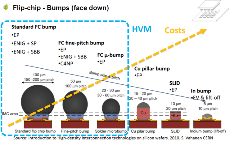
Metzger explained the thermal-mechanical, chemical and electrical effects that complicate the shrinking of bumps. He mentioned weaknesses of thermal compression bonding (TCB) and how direct bonding simplifies contacting wafers and dice. He referenced SET’s current alignment precision (+/- 1µm) and throughput (100s of dice per hour) and highlighted that cleanliness and planarity are key criteria for successful direct bonding.

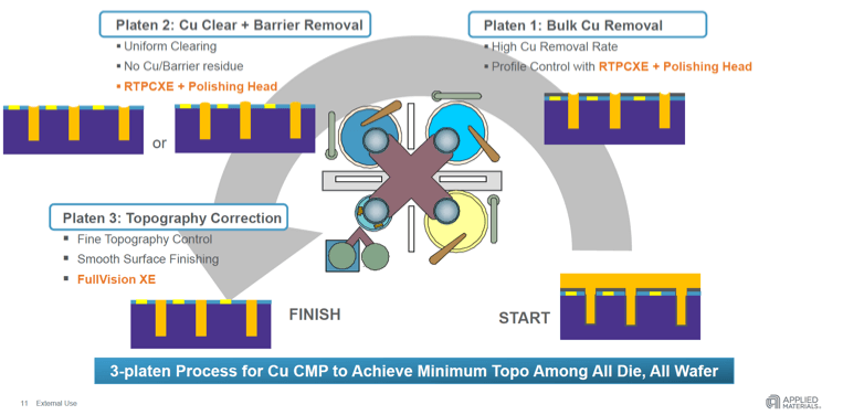
Dennis Ogino from Applied Materials (AMAT) addressed the planarity topic right away and confirmed that it’s a critical challenge. He described AMAT equipment for the backend of line (BEOL) wafer processing, which includes via reveal and chemical-mechanical polishing (CMP). Figure 3 shows the via-reveal steps. CMP uses a similar, multi-step process flow.
Stephen Banik from LAM Research presented LAM’s electroplating capabilities for advanced packaging solutions – the SabreR 3D electroplating platform. As the contact sizes for direct bonding and the line/space dimensions of interconnects continue to shrink to < 1 µm, electroplating becomes more challenging. Banik showed details of how LAM keeps up with these requirements.
EV Groups’ Karine Abadie explained how EVG addresses the challenges shrinking geometries bring. She also mentioned that the rapid growth of monolithic 3D memories (e.g. Samsung’s 3D NAND) causes capacity shortages. Abadie discussed the evolution of the company’s GeminiR product family and emphasized that high-quality materials are of course also essential for high-yielding manufacturing flows.
EDA Design Tools Support
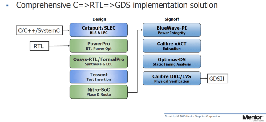
The presentation from Kristian Zoerhoff, Mentor, A Siemens Business, preempted my usual question: “and what’s about design tools support”. First, he outlined Mentor’s current capabilities to minimize power dissipation and heat – the #1 challenge for multi-die integration. See a flow diagram in Figure 4. Then Zoerhoff described architectural, implementation and verification challenges 3D ICs designers face and outlined how Mentor is working to address them, in cooperation with Leti.
Conclusion
This workshop confirmed that it takes the cooperation of many domain experts from companies across the entire supply chain to develop new and compelling technology like 3D-IC. CEA Leti, one of the biggest European R&D organizations, is showing remarkable success in funding and developing multi-die solutions as well as monolithic homogeneous and heterogeneous ICs.
Considering that some of the IC value creation is moving from the die(s) to advanced packaging solutions, I would have liked to also see one of the big OSATs (Amkor or ASE) presenting their contribution to 3D-ICs. Maybe the 7th 3DVLSI Workshop will include more about the design and manufacturing of advanced packages.
I hope to see you at:
- The Microtech Innovation Summit in San Jose from November 5 to 7 to learn about business trends as well as the technical capabilities of MEMS and Sensors. They are the “eyes and ears” that feed data to the high-performance computing devices and make broad AI deployment practical and useful.
- At the MEPTEC Luncheon in Milpitas, on November 13, Tom Dillinger will talk about design challenges at advanced nodes. Anand Joshi will address processing challenges posed by burgeoning AI chipset markets.
- At the 65th IEDM in San Francisco, from December 7 to 11 you’ll get updates about many IC topics.
Thanks for reading….Herb


