
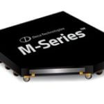
Deca Technologies has confirmed that its M-Series™ fan-out wafer-level packaging (FOWLP) technology has been adopted by Qualcomm for power management integrated circuit (PMIC) devices in Samsung’s S10, the Xiaomi Mi 9 and LG G8 smartphones. (Figure 1).
And in other news, advanced packaging was the Cinderella Story at Hot Chips 2019.
How to Solve Sidewall Chipping

Reportedly, sidewall chipping of conventional fan-in wafer-level chip-scale packages (WLCSPs) remains a key quality concern for cell phone OEMs and IC companies throughout the supply chain. Chipping or cracking defects can arise during device singulation in shipping or in the board mounting process due to the exposed silicon. Adopting M-Series FOWLP mitigates this problem since Deca’s patented structure encapsulates the active semiconductor side and the four surrounding vertical sidewalls of the device (Figure 2).
The Players in the Deca FOWLP Story
Qualcomm has been engaged with Deca/ASE to improve the PMIC side-wall protection with FO packaging. Deca’s M-Series provides a four-side molded protection that can address sidewall cracking of the die.
In 2016 ASE invested $60 million in Deca and licensed Deca’s M-Series™ FOWLP technologies and processes.
As part of the agreement, ASE and Deca have jointly developed the M-Series fan-out manufacturing process and expanded ASEs production of chip-scale packages (CSPs) using this technology. Qualcomm’s new PMIC based on Deca’s M-Series packaging has been adopted in the latest Samsung Galaxy S10 (Qualcomm Snapdragon version 855). In 2018 DECAs M series technology won the 3D InCites device of the year award.
Deca reports that M-Series is built using the chip-first face-up process with a layer of epoxy mold compound (EMC) between solder and die. Qualcomm reports that encapsulation technology has shown superior board-level reliability (BLR) and better results in crack and drop tests. “…this can also be viewed as a stress buffer layer which enables bigger solder balls to be placed at a finer pitch, providing significantly higher reliability. Furthermore, the properties of M-Series’ EMC is optimized, and its mechanical performance is similar to the likes of IC substrate laminate in FC CSP, which is impressive.”
It is reported that the BLR performance of the M-Series is about 3x better than eWLB and fan-in and within a comparable range of thick and thin FC CSP.
Yole Developpement reports:
- Fan-in WLP package typically undergoes a full-function test at wafer level followed by mechanical blade dicing. Such blade dicing may cause either front-side or back-side chipping, which results in yield issues that are not detected before the SMT process. This is exacerbated by thinner die.
- Other Fan-out packaging technologies, such as eWLB (Infineon licensed by ASE, Amkor Europe (former Nanium) and JCET (StatsChipPAC), as a chip-first face-down process does not have an additional layer of EMC between die and solder which results in poorer BLR performance.
- While FC CSP is comparable to M-Series in BLR performance, M-Series allows the mobile applications to go thinner.
Thus even though Deca’s M-Series cost is higher than eWLB and twice that of Fan-In WLP, the yield-cost gain due to improved reliability and quality reportedly exceeds the higher margin in M-Series ASP.
Yole concludes that Deca’s M-Series customer traction is due to its technical value, not any projected cost reduction.


Packaging Key at Hot Chips
There are certain microelectronic conferences that have significantly more prestige than others. On the front end, for decades, researchers have fought to get their latest work into the Hot Chips symposium. Since it started in 1989, Hot Chips has been known as one of the semiconductor industry’s leading conferences on high-performance microprocessors and related integrated circuits. The conference is held once a year in Silicon Valley. This year the conference reportedly drew 1200 attendees. Think of it as being the equivalent of getting your packaging work into the IEEE’s ECTC.
For several years IFTLE has been warning societies like IEEE EPS and IMAPS that front end work was withering as scaling comes to an end, and front end researchers would be moving into what has typically been the realm of the packaging community. In fact, that was the driving force for changing the name of IEEE’s CPMT (components, packaging and manufacturing technology) Society to EPS (Electronics Packaging Society). FYI, Subu Iyer (IBM/UCLA) and I chaired the name change committee for EPS.
I will try to draw a simple analogy for you. Microelectronic Packaging has basically followed the storyline of the famous fairytale Cinderella. To make a long story short, Cinderella had two “evil” stepsisters who got to spend all the money and got to go to all the parties while she was relegated to cleaning up after them. When Cinderella was finally allowed to step into the limelight, she won the heart of “Prince Charming”. I’m sure you get it now….Cinderella is packaging and the evil stepsisters are the front end players who have controlled direction and expenditures for decades, treating packaging like a second class citizen.

Well, the 2019 Hot Chips certainly continued to prove my point. EE Times reports that “Multichip packaging and chiplet technology made its presence felt throughout the conference, with related products and technologies from AMD, Intel, Nvidia, and TSMC. Intel demonstrated a way to pack a full Lakefield PC platform (processor and memory) into an extremely compact package using die stacking technology called Foveros. Lakefield also has a heterogeneous processor configuration with one big x86 CPU core and four smaller Atom cores in one die.”
So get that pumpkin carriage ready to go and get those glass slippers on because it is the Era of Advanced Packaging! If you’re the packaging expert in your company…time to ask for a raise!
For all the latest in Advanced Packaging stay linked to IFTLE…………………………….