
Françoise promised in her recent blog that my ECTC blog would follow shortly. Finally, after attending DAC in Austin as well as the iMAPS’ SiP Conference in California’s Wine Country and shortly before attending Semicon West in San Francisco, I found some time to report what I saw and learned at ECTC 2017 in Orlando. ECTC offered six parallel tracks for the about 1500 attendees. I could of course only attend one of these tracks at a time. See below some info about the topics I find important for the success of system-in-package (SiP) technologies, like 2.5/3D-ICs, FO-WLP, etc.
Before diving into the ECTC topics, allow me to talk about the importance of industry conferences in general: In my 25+ years in EDA and ASIC companies, and additional 15+ years running my own eda2asic company, I have never seen so many reasons for NOT continuing “business as usual”. Mergers and acquisitions of IDMs, fabless IC vendors, and even OSATs are striving for economies of scale and are pooling capital to enable the enormous investments in R&D, manufacturing equipment, and employee education and re-training needed of design and manufacturing experts, to remain competitive.
I find the above events and many other trade conferences to be very useful for educating a company’s most important asset – its people – about new market requirements and available new technology solutions. Especially the now rapidly emerging SiP technologies (like 2.5 & 3D-ICs and multi-die FO-WLP) enable more efficient system architectures and much better performance per Watt. They’ll prove soon that lower non-recurring engineering (NRE) and shorter time-to-market, as well as significant system cost savings, can be accomplished with the wide range of SiP solutions available. However, every company’s engineering teams need to take the time to educate themselves on new market requirements, competitive threats, technology innovations as well as has to invest in build working relationships with new suppliers and evaluate their strengths.
Out of six parallel ECTC tracks, covering more than a dozen packaging technology areas, I spent most of my time learning about these topics: “Fan-out Packaging Process”, “Interconnect Advances”, “Integration and Reliability”, “Reliability Challenges in 2.5D/3D Interconnects” and “3D Cu-Cu and Micro-Bump Bonding Technologies”. In addition to joining many sessions, I also spent time on the exhibition floor, primarily with experts from large assembly houses (Amkor, ASE, StatsChipPAC), Universities (Binghampton, GeorgiaTech), EDA vendors (Cadence, Mentor – A Siemens Business as well as Zuken) and several IC packaging materials suppliers.
Session One focused on Fan-out Packaging.
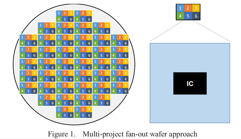
Knowing how important multi-project wafers (MPWs) are for low-cost SoC prototyping, I wanted to hear what Tanja Braun from Fraunhofer in Berlin had to say about the capabilities of their platform for FO-WLP prototyping and low-volume production using their 200mm line. As expected, a common package size is needed, but die sizes and thicknesses can vary. Common process parameters and materials, suitable for all designs on the wafer, are of course mandatory. Braun suggested that a mask-less RDL approach (=direct laser imaging) may be better than the current techniques. Figure 1 depicts such a multi-project fan-out wafer.
The following speaker, Joungrae Kim from Amkor Korea, talked about their silicon-less integrated module (SLIMTM) packaging technology, offering sub-micron redistribution layer (RDL) capability. Using an inorganic interposer and a 65nm process, SLIM can offer up to ten thousand I/Os, typically one and up to tw0 RDL layers in this chip-last /self-aligned process. The minimum bump pitch of 30µm is essential to enable such a high I/O count.
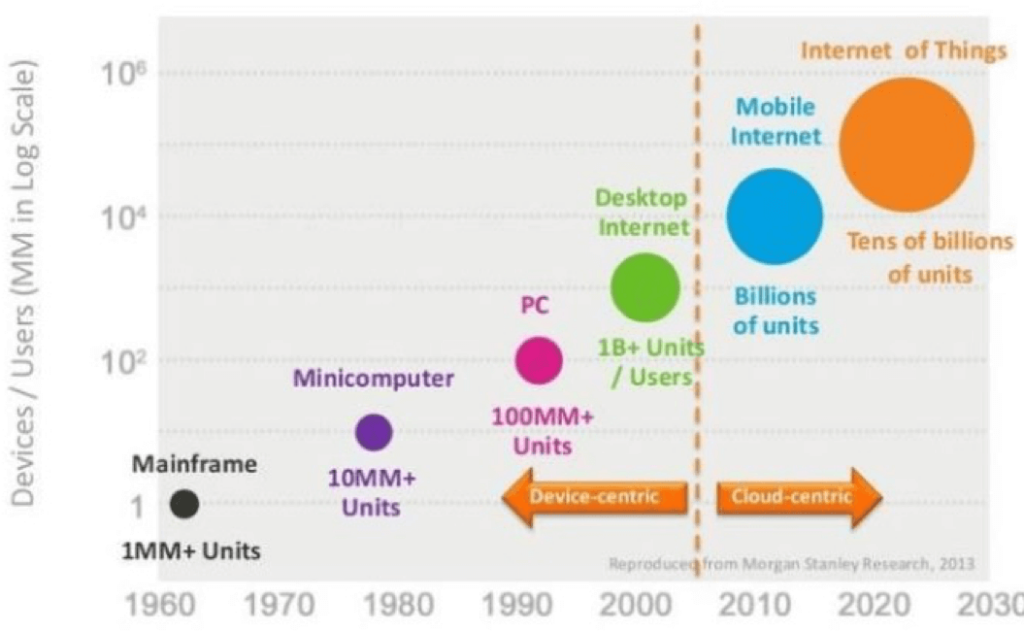
Andre Cardoso from Nanium (soon to be officially merging with Amkor) introduced his message with a diagram of computing trends from Morgan Stanley (Figure 2), then he described the die first, face down high-density FOWLP system integration solution Nanium has developed for single die and vertically stacked multi-die designs with only 0.5 and 1mm package height, respectively.
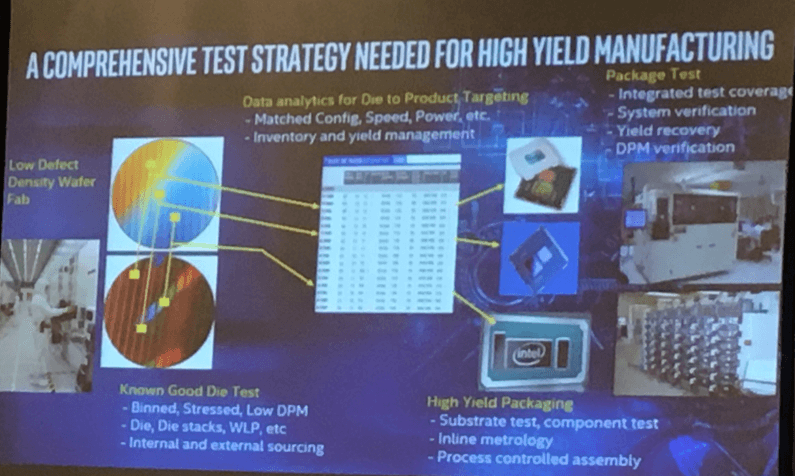
Wednesday’s impressive lunchtime keynote speaker was Babak Sabi, Corporate VP and Director of Assembly and Test Technology Development at Intel. He conveyed a lot of optimism, but also a key weakness of the current multi-die IC offerings. He summarized his message with the slide in figure 3.
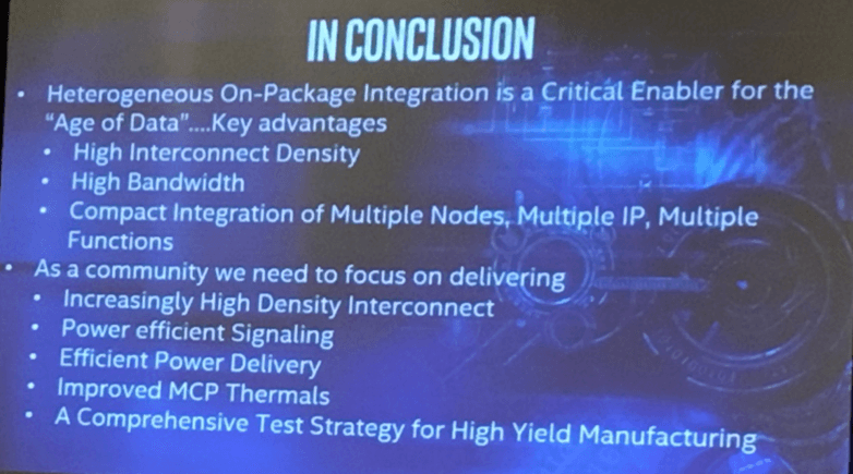
All these topics are of course important and need to be addressed. From my perspective, the most critical one is the last point on this slide: a test strategy for high yield manufacturing. That’s why I organized that a significant part of this year’s Electronic Design Process Symposium (EDPS 2017). It will be held in Silicon Valley on September 21 and 22 and will focus on SYSTEM-level Test (SLT). EDPS 2017 will also address how to use artificial intelligence (AI) and machine learning (ML) for IC design and manufacturing/test. If you are interested or even responsible for improving the quality of your company’s ICs, please join us at EDPS 2017.
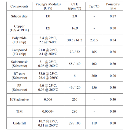
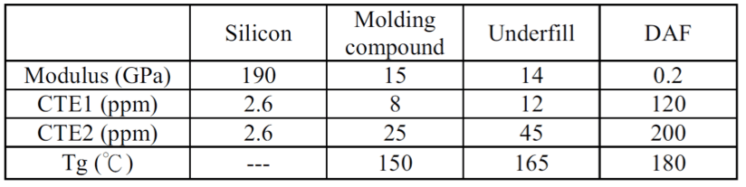
Ian Hu from ASE started the afternoon session on Wednesday with a reliability analysis of a fan-out chip on substrate. Because the thermal-mechanical material characteristics impact the reliability of a device significantly, Hu showed table 1 below with essential material characteristics. He also stated that ASE has developed a methodology for warpage simulation and reminded us those accurate models are absolutely needed for meaningful simulation results.
ITRI’s Wen Wei Shen presented a process for TSV-less interconnections for FOWLP, based on Infineon’s eWLB technology. ITRI, Brewer Science and Corning jointly developed this process, shown in Figure 4. Shen also mentioned that they plan to migrate this chip-on-wafer technology to panel processing.
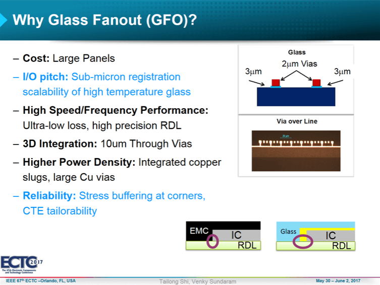
The Georgia Institute of Technology has been working with glass suppliers on advanced packaging technologies for several years already. GIT’s Venky Sundaram demonstrated a joint development with Disco and Schott, using glass panels for large dies with high I/O density, targeted for high-frequency multi-chip designs. This process offers 1µm L/S and allows a large ratio between the die(s) and package size. Also, the development partners target to enable vertical stacking of such designs. Figure 5 below shows important benefits of glass fan-out technology.
Whenever I had time to walk the exhibition floor, I was very happy to see Cadence, Mentor/Siemens and Zuken demonstrating their commitments and support for planning, design, verification, failure analysis and debug of multi-die ICs. Best of all, I often saw my friends from OSATs, in discussions with these EDA experts. The cooperation between EDA vendors and manufacturing/test houses is ramping up – finally!
My Thursday morning started with a presentation from STATS ChipPAC’s Seung Wook Yoon about their capabilities and success with large embedded Wafer Level BGAs (eWLB). Yoon talked about the transition to Cu-Cu pillars, efforts to reduce L/S pitches from 5/5 to 2/2µm, benefits of fan out versus flip chip packages and emphasized that more and more discrete components (RLC) are being deployed inside these IC packages.

Qualcomm’s Ray Alvarado showed results of a board-level reliability (BLR) study they performed, using a 28nm RF design, SAC 405 solder balls and no underfill. Especially for corner balls, it is very critical how all the ball get arranged, to achieve reliable connections using only 0.35mm ball spacing.
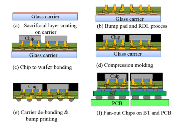
ASE and BOSCH presented a joint wafer-level platform development project for complex MEMS sensors to be used in automotive, consumer and IoT applications, where both footprint and package height need to be minimized. Chip to wafer assembly turned out to be the most attractive solution for achieving the required electrical performance as well as mechanical stability and repeatability. Warpage of the 100micron thin die, the TSV reveal step, thin wafer handling (using glass carriers), were some of the challenges to resolve.
In the Additive Manufacturing session on Thursday afternoon, TU Dresden, Leti and Michigan State University presented their research in this very promising field. Dresden addressed how additive manufacturing can be used for FOWLP prototyping, Leti showed how flexible and customizable 3D printing can be and Michigan State discussed how high-frequency coaxial transmission lines can be printed.
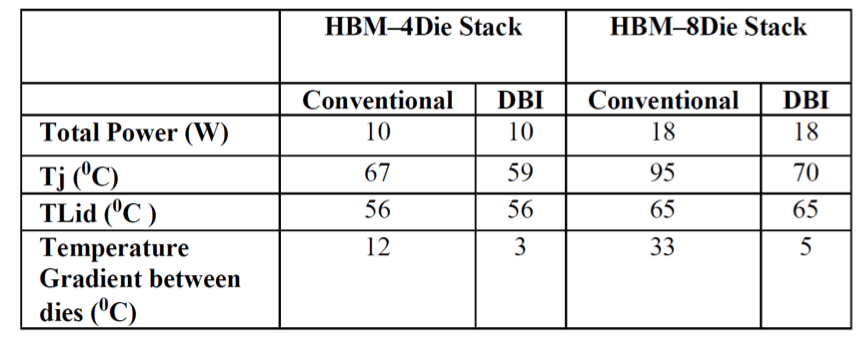
Javier De La Cruz from Invensas presented the benefits of their very fine pitch direct bonding interconnect (DBI) technology for image sensor, MEMS, RF filter and 3D memory applications. In addition, DBI eliminates the need for underfill. It significantly improves thermal conductivity between vertically stacked dies. See Invensas thermal simulation results in Table 2, below. It compares thermal characteristics of conventional micro-bumps with DBI, using as an example, the widely used high bandwidth memory stacks.
SPIL’s Chieh-Lung Lai presented a warpage study, using a 30 by 40mm interposer and two very large dies, each 20 by 25mm, using die-attach film (DAF). He outlined the process flow, explained how SPIL can calculate warpage and discussed a table of important material characteristics and glass transition temperature.
Laurene Yip presented a board-level reliability study performed by Xilinx. They mounted very large IC packages, containing 45mm interposers with through silicon vias (TSVs) and very large, thinned dies on a Megatron 6 board to analyze after how many temp cycles solder ball fatigue would lead to cracking of the SAC 305 balls.
Xilinx varied package parameters and assembly steps and saw first failures occurring after 1600 to 3000 temp cycles from 0 to 100°C.
On Friday morning Ganesh Hariharan presented another reliability study Xilinx performed. He proudly reminded the audience that Xilinx has used TSMC’s CoWoS process since 2012 in volume production and achieves higher than 90% yield with their complex FPGA devices. This reliability study analyzed low K cracking, micro bump failures due to aging, underfill delamination, TSV, and C4 bump failures and achieved satisfying results.
Last, but certainly not least, let me again highlight test as an area of concern and issue a call to action. SiP technology is exactly what the word says: A SYSTEM in a package, and needs to be tested like a system. Design for test, accessibility, traceability of the building blocks, self-test, redundancy and other needs need to be given more attention than I can see currently.
I am in good company with my concerns about the relatively slow progress in multi-die IC TEST technologies.
See in Figure 6 below another slide Babak Sabi, Intel’s VP for Assembly and Test, presented during his keynote:
Enjoy your summer break and take a few minutes to read my blog about Semicon West, from July 11 to 13. ~ Herb


