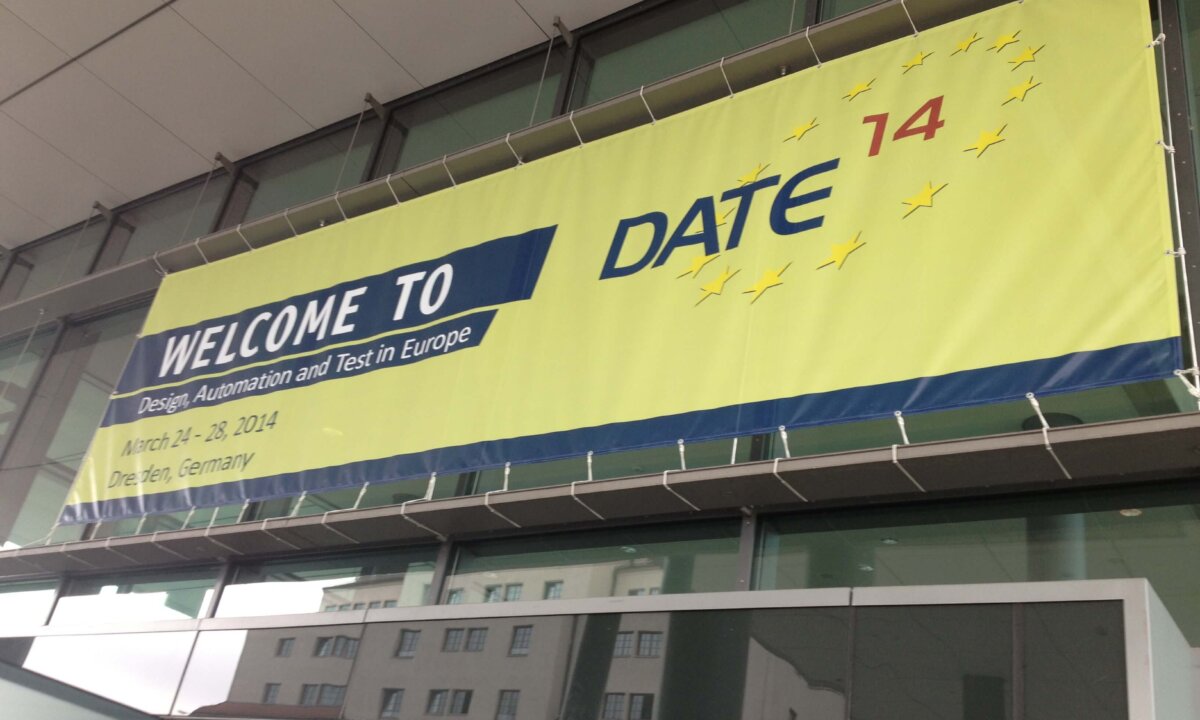
Design and Test Europe 2014 (DATE 2014), which took place in Dresden, March 24-28 2014, brought together semiconductor design and test engineers from all over Europe and around the world for the purpose of understanding the latest trends, methodologies, and technologies being developed to address the ever-changing needs of chip design and test for the semiconductor and microelectronics industry. This year’s message was loud and clear: it’s time for a collaborative semiconductor supply chain to take us to next-generation technologies.
This was the first time I ever attended this event, because I had been asked to moderate a panel discussion for the Friday Workshop on 3D IC Integration, and my first impression was that, other than those who had invited me to participate, I hardly knew any one in attendance or exhibiting. I point this out, because when I attend conferences that have anything to do with 2.5D and 3D IC technologies, processes and manufacturing, I know most of the people in the room, and they know me. This was a good illustration of the line that still exists between the chip design community and the semiconductor manufacturing community. And it’s this line that must be rubbed out in order for the co-design and co-development that is needed to bring 3D integration technologies to market.
I also discovered that unlike other industry events that either have tracks and sessions devoted to 2.5D and 3D IC technologies, or are devoted entirely to 3D architectures, the attendees of DATE 2014 are not yet completely convinced that 3D integration is an alternative to tradition scaling and more complex SOC architectures. Case in point: I was asked at the last minute to moderate an executive panel on the increasing complexity of SoC designs, and I came armed with my one –and-only question: what do you think about the idea of partitioning complex SoC designs into simpler functionalities and stacking them to create 3D SoCs for improved performance and lower power? Rather than the nods of agreement I expected, I was met with a negative response. Rainer Kress, of Infineon, explained that in his area of automotive electronics, despite the complexity of SoC designs, it was still simpler to work with single chips in a package, and that it would be more complicated to stack the different functioning chips.
This was not what I expected to hear, especially having just come from a keynote presentation by Gerd Teepe, of GLOBALFOUNDRIES, who talked about increased foundry costs due to shrinking nodes and the increasing costs of lithography. He noted that while the cost of the fab is going up, output is going up as well. However, the cost of the technology itself may limit development.
He also spoke of the complexity of SOC designs, and that what is needed is a SOC-optimized technology architecture focused on enabling SoC level power management. He talked of the issue of “dark silicon” which refers to spots on a chip that could compute, but don’t because of power, and this is a problem that could be solved with design.
While he didn’t discount the advantages of leading-edge nodes (eg. a 14nm modular FinFET platform for Extreme Mobility) he said these next-generation transistor architectures (3D silicon) are “terribly complicated” and have tremendous design implications. “A complete SoC solution is based on deep collaboration with EDA, IP and customers,” he said. He also spoke of 2.5D and 3D supply chain enablement that links OSAT partners to GLOBALFOUNDRIES offerings that includes EDA and IP partners for development and validation; GLOBALFOUNDRIES for front-end CMOS silicon; memory partners for integration and characterization; and bump and probe shared by GF and OSATS partners.
Ultimately, he called for a semiconductor supply chain transformation that transfers process complexity to the design space in a collaborative design ecosystem. “What makes our jobs so joyful is not only carrying the design complexity piece bus also carrying the process complexity piece,” he said. “There is a trend for more collaboration in the ecosystem rather than less, which makes for a more colorful job as we increase interaction with more intelligent people feeding the supply chain.” GLOBALFOUNDRIES calls shift “Foundry 2.0” that offers customers open, flexible, and cost effective supply chain.

I was relieved to see the benefits of 3D IC for SoC partitioning come up again during the session, “The Bridge between Moore and More than Moore.” In this session, several speakers discussed the design technologies for 3D integrated systems, including both 2.5 and 3D designs. According to Andy Heinig, Fraunhofer IIS/EAS, one of the keys is to compare all the possibilities early on in the system, because of the increased complexity of the design space. Chip design is already complex, but with 2.5 and 3D design there are multiple design spaces due to the structural complexity that comes with package design that is multi-scale, multi-physics, and exceeds the capacity of current simulators. Now there are electrical and thermal issues to address. The key? Collaboration between system architects, component designers, IC manufactures and the OSATS. Heinig noted that Fraunhofer IIS/EAS has developed a flow and tools that allow development from specifications to the 3D products.

Infineon’s Jochin Reisinger cautioned attendees to pay attention to requirements of what he termed “fractal architectures” – a system that is or can be seen as a subsystem. “We are still far away from having an effective/efficient design flow to enable the development of complex 3D systems,” he said. “Fractal architectures are not covered. Mainly the management of significant, but still so-called 2nd order effects are not supported adequately.” He also says that too many 3D technologies are developed in parallel. Better alignment would support our competiveness. An actual 3D system is used mainly for high-speed memory oriented application, which isn’t significant for Europe. Rather, he sees EU alignment with new application fields of e.g. bio and medical fields ask for new materials and system architectures.
On the up side, Reisinger sees that national and international (EU) collaborations have brought the 3D community together, and the leading EDA vendors are offering “some nice, helpful features.” While Europe is clearly headed in the right direction, there is still work to be done, and the call for collaboration is stronger than ever. ~ F.v.T.


