
As much as the industry is intent on holding 3D technologies to a narrow definition, I’m compelled to remind readers that before 3D had to include a TSV interconnect to be considered a 3D technology, and before the term 2.5D had been coined, 3D packaging was already being touted as a value-add way to accomplish improved performance and form factor issues. At SEMICON West, I met with executives from two companies that currently offer 3D solutions while also working on development of what purists refer to as “true” 3D ICs.
Bridging the Gap
While we’re waiting for 3D ICs to become commercialized, there are products TODAY that require the performance, low power, and high bandwidth solutions that 3D ICs promise to provide. Invensas, a wholly owned subsidiary of Tessera Technologies, is addressing that gap with two product families that leverage the current infrastructure today, while also investing “millions” in developing 3D ICs technologies that will meet the 2015 target. I’ve written about both product families that Invensas has launched in the past year, the xFD and the Ball Via Array (BVA).
The former is a 2D package, while the later is a PoP configuration, so is officially considered 3D packaging. Both leverage wire bond technologies in a novel way to shorten interconnects, and in the case of BVA, to increase the I/O connections. Simon McElrea, CEO, Invensas, shared some product updates. With xFD, Invensas has engaged customers on both server platforms and client platforms for notebooks and tablets. BVA, just launched last month at ECTC, is still in partnership mode, working towards high-volume readiness mode. With 3D TSVs, he says the vast majority of R&D investment is going into 2.5D and 3D. The company is building the internal infrastructure to support that, explained McElrea, but they don’t expect it to be revenue-generating for another 3 years or so.
Power and Analog 3D
Texas Instruments has a broader definition for 3D technologies than the industry at large because the IDM has a broad product portfolio that includes power and analog devices. Dave Stepniak, Packaging Manager, explained that at TI, 3D is a combination of miniaturization and integration.
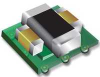 For example, the company’s MicroSiP is a 3D integrated power and analog device that involves embedding a PicoStar chip in an organic substrate, with passives mounted on top to create a DC/DC converter embedded picostar embedded in substrate. TI Fellow, Dr. Sreenivasan Koduri, explained this is a flexible mix-and-max configuration that allows for the integration of die, passives and/or sensors. This product is in high volume manufacturing at TI, and is found in mobile applications. It reduces power density by 50% and is a complete power supply, so there’s no need to worry about designing a power circuit.

Another example is TI’s Power Block that stacks a copper leadframe, FET, a clip, another FET, and another clip. This device targets high current applications. Heat movement is extremely efficient because the copper leadframe handles both current and heat, and handles lots of power. This is how 3D technology is being used in power FETS, explained Stepniak. TI’s message? TSVs aren’t the only way to do 3D, and you have to choose which is the best application for each space.

While 3D purists may object to broadening the definition beyond strictly 3D silicon, I think it’s important to remember that 3D is a complete area of technology that at the system level, can include the board, package and silicon; and that TSV all by itself is not 3D, it is a 3D enabler. ~ F.v.T.


