
CEA-Leti today announced the launch of a major new platform that provides industrial and academic partners with a global offer of mature 3D innovative technologies for their advanced products and research projects.

To help its partners solve key technology challenges, Leti’s Open 3D(TM) global offer includes 3D design, layout, technologies including interconnections, TSV and components assembly, reliability tests and final packaging for components or systems achievement.
The Open 3D(TM) platform includes Leti’s proven “off-the-shelf” 3D technologies that provides decisive advantages in performance, form factor and cost for a wide range of markets like bio/medical, aeronautics and space, consumer applications, defense and security, or fundamental research.
The platform enables customers to achieve proof of concept with a small quantity of wafers or prototyping with a larger quantity. The offer is based on limited mature technologies in order to ensure moderate costs, short cycle times and performances corresponding to the initial technical requirements of Leti customers.
Open 3D(TM) also operates directly on active wafers with embedded components or on passive wafers for interposer technologies.
“Open 3D leverages Leti’s proven 3D expertise and infrastructure for colla borations that address new applications and markets, as a key new part of Leti’s mission to create innovation and transfer it to industry,” said Laurent Malier, CEO of Leti. “Our partners will include laboratories, universities and international research institutes as well as fabless chip companies and niche market manufacturers and integrators.”
Operated on the Minatec Campus in Grenoble with Leti teams and technological platforms, Open 3D(TM) is fully operational for 200mm wafers and will be operational in 2012 for 300mm wafers. Modules offered in the platform’s technology catalogue include:
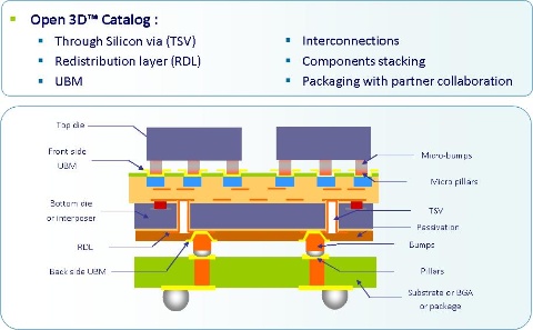
— Through silicon vias (TSV) with aspect ratios to 1:3

— Interconnects for chips to wafers based on micro-bumps technology
— Interconnects for chips to substrates based on bumps technology
— Redistribution layers (RDL)
— Under-bump metallurgy (UBM)
— Temporary bonding, thinning and debonding
The technology catalogue will be regularly enriched with new technological modules that correspond with new 3D mature technologies and customer requirements.
Visit Leti’s Open 3D page to learn more about participating in this collaboration.


This appears to be a good alternative to Tezzaron or even TSMC which recently announced a complete ecosystem for 3DIC stacked products. The flow defined by Leti’s Open3D Offer seems to be complete, ideal for a small player who can be innovative with the 3DIC stacking.
The question I have is -what is Leti’s model for transfer to high volume manufacturing? Outside of TSMC, I haven not come across any one defining and owning a significant (if not complete) part of the supply chain. So where does one go for a ‘copy exact’ of the recipe for their 3DIC?
MP Divakar
Hi MP –
I’m actually scheduled for to interview David Henry at CEA-Leti on Monday, and will pose this question to him. Stay tuned!