
SEMATECH’s 3D Enablement Center (3D EC), together with the Semiconductor Industry Association (SIA) and Semiconductor Research Corporation (SRC), has identified the top technical challenges for new “killer” applications to enable future development of heterogeneous 3D integration beyond mobile wide I/O DRAM.
Following the introduction of the wide I/O DRAM, further research and development of 3D IC technology will be driven by high demand, high volume applications that continue to demonstrate the benefits of 3D integration, including lower power consumption, higher performance, increased functionality, and lower cost.
Since January 2011, SEMATECH’s 3D EC has spearheaded the development of standards and specifications for 3D. To prepare for the future 3D integration ICs and systems, the 3D EC is identifying 3- to 5-year window killer applications and the common technical challenges they pose to smoothly extend 3D technology beyond mobile wide I/O DRAM.
Discussions with expert university professors and diverse users, including the 3D EC member companies and SRC, have identified heterogeneous computing, memory, imaging, smart sensor systems, communication switches, and power delivery/conditioning as some of the potential future killer applications. Additionally, the common technical challenges associated with these applications have been prioritized: lowering the cost of 3D architectures, system/architecture pathfinding, generic heterogeneous multi-die stack testing issues, and thermal management.
“Tackling the common challenges of next generation applications is critical for acceleration of the broad adoption of 3D ICs,” said Dan Armbrust, president and CEO of SEMATECH. “SEMATECH’s 3D Enablement Center’s goal in the next phase of this broad based collaborative program is to provide the enabling infrastructure to address these common technical challenges.”
“SRC has extensive university programs and expertise, and we are eager to employ these resources and help the industry address such challenges as lowering the cost of 3D structures, thermal management concerns and complex testing issues,” said SRC President Larry Sumney. “Combined with SEMATECH’s existing efforts in developing 3D technologies, we will pursue an ambitious effort to enable the commercialization of 3D ICs.”
“The development of 3D integration technology is at an inflection point,” said Brian Toohey, president of the Semiconductor Industry Association (SIA). “The industry has experienced the benefits of collaboration in many efforts, from the semiconductor roadmap to finding the next switch. This evolving partnership aims at taking 3D integration technology to the next step – to fully realize its significant potential for semiconductor manufacturing and design.”
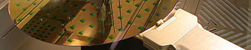
SEMATECH’s 3D Enablement Center is a cooperative effort among members of the program, the SIA, and the SRC. Since its launch in December 2010, the center has focused on enabling industry-wide ecosystem readiness for cost-effective TSV-based 3D stacked IC solutions. The initial set of activities encompassed working with critical standards development organizations to set 3D standards, especially for inspection/metrology and bump metallurgy. During 2011, the 3D EC expanded its efforts to include activities that would address pathfinding electronic design automation (EDA) tools and complex test vehicles.

Membership is open to international fabless, fab-lite, and IDM companies; outsourced semiconductor assembly and test (OSAT) suppliers; and EDA process tool and materials suppliers. In addition, the program and its members are collaborating with a broad network of companies, consortia, universities, national laboratories, and associations from around the world.


