

The annual International Electron Devices Meeting (IEDM) presents the latest developments in electronic device technologies focused on advanced scaling, heterogeneous integration, quantum computing, and wide bandgap devices. Among several excellent papers on 3D integration were two papers on 3D sequential integration, long the holy grail of 3D integration because of the promise of up to 50% logic-area reduction. Additional benefits are the reduction in interconnect length, and heterogeneous integration of materials other than silicon, e.g. Germanium (Ge) or compound (III-V) semiconductors.
3D Stacked FinFETS
Anne Vandooren, of IMEC et al, presented “First Demonstration of 3D Stacked FinFETs at a 45nm Fin Pitch and 110nm Gate Pitch Technology on 300mm Wafers”. The principal challenge of 3D sequential integration is the management of the thermal budget of the top tier to avoid degrading the bottom tier. In this work, finFET devices are processed with temperatures as low as 525°C. The top devices are junction-less devices with channel doping set prior to top silicon layer transfer. The process flow is shown in Figure. 1.
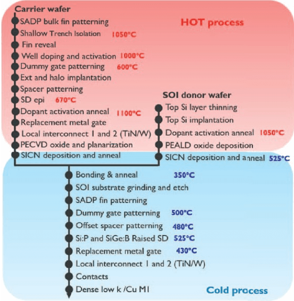
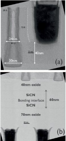
The bottom devices are processed using a high-k last replacement metal gate and two layers of tungsten local interconnect. The doped top Si layer is then transferred onto the bottom device layer by wafer-to-wafer bonding using oxide planarization followed by SiCN to SiCN bonding. FinFET devices are then processed in the top Si layer with a fin height of ~40nm and a width of ~10nm and a minimum gate length of ~ 24-30nm using a spacer-defined double patterning process. 3D stacked devices, as well as silicon-on-insulator (SOI) devices, were processed using the same low-temperature process.
Top layer transfer by bonding while maintaining good yield is a principal challenge. A minimum amount of oxide removal is necessary to avoid pattern-related voids, first appearing near the edge of the wafer.
Top-tier nMOS device Ids vs Vgs characteristics are well behaved for both long and short channel devices. When a dipole layer of 0.2nm LaSiOx was inserted in the TiN/HfO2 gate stack, Vth was lowered from ~0.62V down to ~0.38V.
Junction-less devices showed improved PBTI reliability compared to inversion-mode reference devices. Combining junction-less devices with the LaSiOx dipole provided further BTI reliability at low temperature.
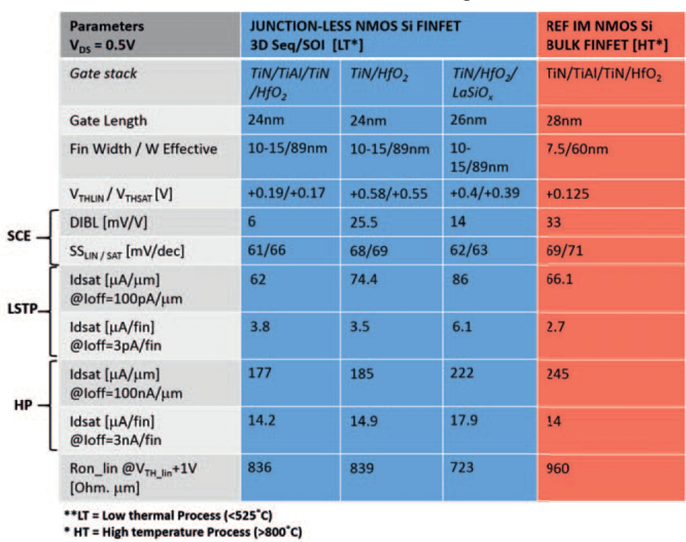
Benchmarking of low-temperature devices vs. high-temperature devices for LSTP applications showed similar or better on-state current while for HP applications, they showed up to 25% on-state current reduction. Further improvement in the HP device can be obtained by increasing the active doping level in source/drain by laser annealing. Benchmarking of low-temperature top tier junction-less devices vs high-temperature bulk inversion-mode devices is shown in Table I.
Breakthroughs in 3D Sequential Technology
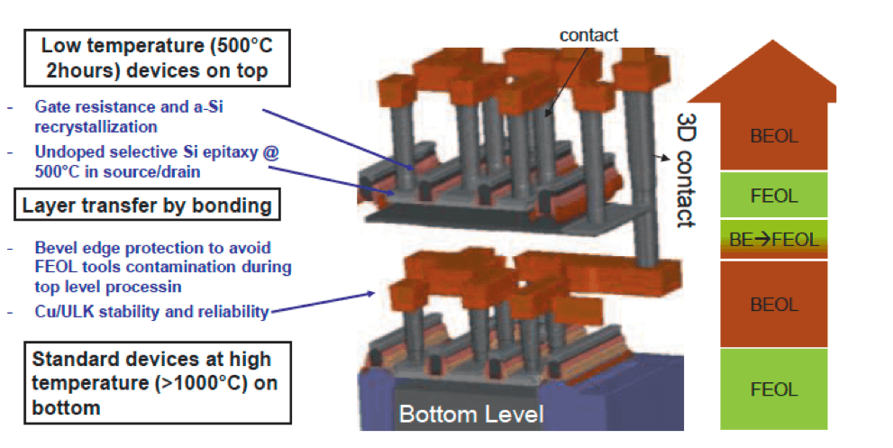
Maud Vinet of Leti, et al, presented the second paper in this session, “Breakthroughs in 3D Sequential Technology”. The requirement of 3D sequential integration for limited top-tier temperature processing poses a number of challenges for both top and bottom tier processing, primarily limiting the top tier thermal budget to 500°C (Figure 3). Critical processing issues are low-temperature gate stack integration and low-temperature selective epitaxy of silicon on source and drain. To enable a higher level of integration, local routing is needed in the bottom layer, but Cu interconnect in the bottom layer can cause contamination when the top layer is reintroduced to the front-end-of-line (FEOL). Ultra-low-k (ULK) dielectric stability of the intermediate back-end-of-line (BEOL) is required for stable top wafer bonding.
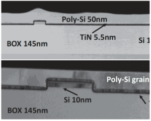
Low gate resistance with good reliability is needed in a gate-first scheme, but neither the crystallization of the amorphous Si nor the dopant activation can be achieved at 500°C. This is resolved using UV nanosecond (ns) laser anneal with a pulse duration of 160ns after deposition of amorphous Si on 5nm TiN/2nm HfO2 followed by chemical mechanical planarization (CMP) to remove surface roughness (Figure 4). Crystallization of the amorphous Si into poly-Si and low sheet resistance were achieved at high temperature (>1200°C) by UV-NLA while not increasing the thermal budget of the bottom level.

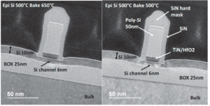
Low-temperature Si epitaxy is sensitive to the control of contaminants, exponential decrease of growth rate, and lower epitaxial layer quality with temperature. Surface preparation included Hf/HCl clean, Siconi NH3/NF3 plasma treatment and a 500°C bake. Selective epitaxial growth showed excellent etch selectivity of amorphous-Si vs single-crystal Si, shown in Figure 5 comparing 650°C vs 500°C H2 bake.
In the iBEOL on the bottom tier, Ti, TiN, W, Ta, TaN, and Cu are deposited on the wafers before being re-introduced into the contamination-free FEOL, presenting a contamination-control challenge. The backside can be easily decontaminated but the materials on the front side need to be encapsulated, but this is not sufficient at the bevel edge, requiring bevel edge polishing and etching to remove contaminants.
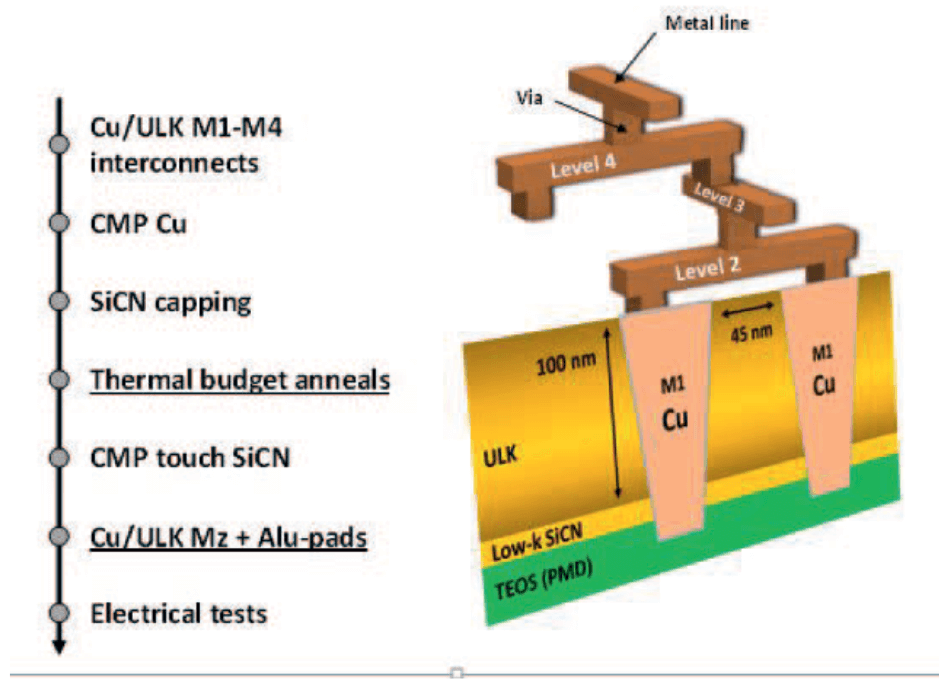
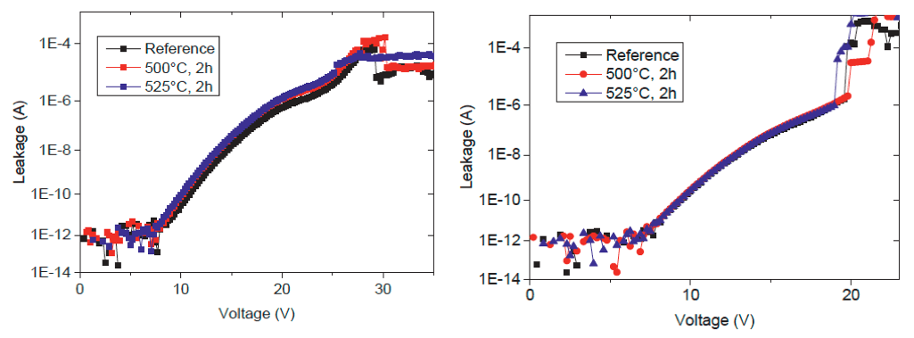
Thermal stability and reliability of the Cu/ULK iBEOL were tested for line-to-line and via-to-line referencing 28nm FDSOI rules as shown in Figure 6. The ULK material was 100nm porous SiOCH, (k=2.7), with a SiCNH etch stop layer (k=5.6). Four metal lines/vias were encapsulated with a SiCN layer for testing. The breakdown voltages for line to line and via to line were stable with insignificant degradation for 500°C anneal as shown in Figure. 7.
DR Cu/ULK BEOL).
Bonding on the Cu/ULK iBEOL was tested with four metal lines, SiCN capping and a 120nm planarized oxide on top bonded to an oxidized bulk silicon substrate and annealed at 600°C and showed good stability. As an alternative to direct bonding of an SOI wafer followed by etch-back, a Smart CutTM was used to transfer a thin Si layer onto the 300mm CMOS wafer, shown in Figure. 8.
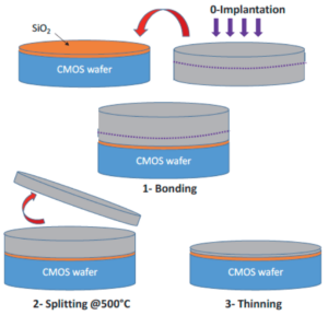
above CMOS wafer. Splitting done at 500°C.
The manufacturability of 3D sequential integration iBEOL with standard ULK and Cu metal lines has been advanced by limiting the thermal budget to 500°C. High-performance top fets have been achieved using UV nanosecond laser recrystallization of doped amorphous silicon and low-temperature epitaxy. A bevel-edge contamination containment strategy enables wafer re-introduction in top tier FEOL after bottom tier BEOL metallization. Compatibility of a Smart CutTM process was demonstrated. Manufacturable 3D sequential integration enables a significant increase in density as well as heterogeneous integration with wide application.


