
“Those who cannot remember the past are condemned to repeat it” ~ George Santayana
Over the past forty years, the presence of legally protected Intellectual Property (IP) has dramatically grown in the processes of electronic system development and deployment. Teams that use IP in product design and/or in subsequent product deployment and support have the additional corporate responsibility to understand the legal and financial trade-offs these design and support decisions make on a corporation’s “bottom line”. Ignorance or miss characterization of these legal and financial factors put a corporation’s product portfolio, developed with good engineering practices, at risk in very competitive and rapidly moving marketplaces.
History
Back in the late 1970’s, silicon microcircuit development was still an immature art where various design communities across many corporations pressed hard to develop new methodologies that could compact more functional circuits into a single silicon die while, at the same time, reduce the cost to manufacture said die. In 1980, Bill’s first job was as a product engineer at Mostek in their Microcontroller group. Product Engineers focused on the myriad of factors that drove yield and costs of the manufacturing processes Mostek products depended on. Just as Bill started his career, he saw a revolutionary new manufacturing process come out; self-aligned gates with ion implantation. This radically different design methodology dramatically disrupted product design and silicon die/wafer manufacturing. The old gas diffusion that required hours to dope a silicon substrate was replaced by an ion beam that quickly ‘hurled’ ions into the silicon crystal structure affecting the electrical properties. The upside was improved gate alignment reducing gate capacitance, reduced time to manufacture while improving yields, doping variations and costs. The downside to ion implantation was increased crystalline damage that required a temperature annealing cycle to heal the structure: but the anneal time was considerably shorter than what the diffusion process required before. Given these advantages, the entire industry quickly adopted this new methodology. But an unexpected issue soon surfaced: a patent2 owned by Hughes Aircraft. Shortly after the patent was granted, Hughes contacted all semiconductor manufacturers to license their patents for royalty payments. Many companies agreed to pay the royalties while Hughes took some to court for patent infringement.
All companies quickly learned how valuable a patent could be in protecting their intellectual property.
Patent licensing offers a new revenue stream to the owner; is a competitive advantage for their products; can be used to deny competitors the rights to sell their products and patent portfolios provide bargaining ‘chip’ to help resolve infringement suits.
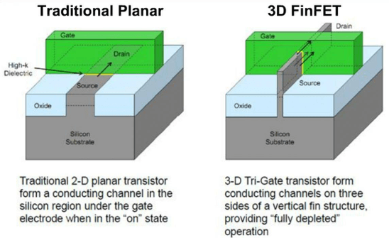
Is history going to repeat: FinFETs, the new >self-aligned gate?
FinFETs made a huge ‘splash’ a few years ago solving the performance issues continually arising while using planar, self-aligned gates. Rather than using a planar transistor, the transistor is now 3D (Figure 1).
A recent article discussed KAIST’s (a South Korean research university) legal suit against Samsung, Qualcomm, and GlobalFoundries over a FinFET patent granted to KAIST. Previous to the legal suit, Prof. Lee Jong-ho, Seoul National University who was in partnership with KAIST, presented to both Samsung and Intel his KAIST enabled FinFET research. Samsung has a foundry partnership with GlobalFoundries. While Qualcomm is a customer of Samsung and uses FinFETs in their silicon design processes. Intel has already agreed to license KAIST’s patent giving KAIST some credibility in this lawsuit. Interestingly, TSMC is one foundry that produces FinFETs that has not been named in either a legal suit or an agreed royalty model (similar to Intel). Given that TSMC is the largest foundry, I am sure that KAIST either has or will approach them to license.
Since Qualcomm is an end customer and not a manufacturer of FinFET technology, one wonders if Qualcomm will pay anything. IF Qualcomm’s infringement is upheld, this could lead to numerous lawsuits for any company that has designed silicon using FinFETs including IP providers or EDA companies that support FinFET technologies: in effect, a ruling and precedent that would impact much of the high technology ecosystem.
Unlike companies that can ‘barter’ patent portfolios against each other to settle disputes, KAIST is a university that produces research with or without partners and then patents the results of their research. KAIST does not generate revenue from manufacturing products but rather validating ideas. If the accused infringers are found guilty, financial ($s) agreements will most likely be the only method to resolve the dispute. KAIST is not a unique entity but is similar to ALL universities that perform research guided by their faculty as well as MS and Ph.D. candidates. Once a novel idea has been proven, most universities quickly patent their ideas hoping to license or sell their patents.
Repeating the future again: 3D structures enabled by TSV or Monolithic processing?
Tezzaron and Monolithic 3D have different methods to create 3D structures. Tezzaron uses thinned wafers interconnected with thousands of small TSVs while Monolithic 3D creates two active (device) layers in the same silicon wafer using ‘normal’ interconnect metal between the two layers. Tezzaron can stack multiple wafers while Monolithic 3D, at this time, only shows two active layers per wafer. In theory, you could add TSVs to Monolithic 3D and stack four wafers to provide 8 unique device layers ( an equivalent of stacking eight Tezzaron wafers). In either solution, performance is gained by shorter interconnect (re: RC effects) using ‘old’ planar process rather than a 3D FinFET. These companies’ respective technologies (Tezzaron and Monolithic 3D) do not need to chase the smaller nodes based on FinFETs (10nm, 7nm, etc) that require higher costs. These alternative lower cost solutions can be a perfect solution for many companies unable to afford the higher cost FinFET based solutions.
But Tezzaron’s and Monolithic 3D’s disruptive technologies represent a similar situation as the self-aligned ion implanted gate and the FinFET: both companies have patented their advancements and as their technologies continue to mature may find a sizeable customer base unwilling to pay for the use of FinFETs related IP.
Will the industry learn to license either of these technologies before they start to adopt them?
If history repeats itself, then the answer will be no. Other companies will try to work around these patents for their own solution (and possible patents), hope to fly under the radar and defend themselves if required. But just like the self-aligned gate and the FinFET scenarios, conquering a market disruption motivates adopters to promote their successes in advertising as well as technical and marketing papers. All these communication mechanisms serve to help a patent owner track potential infringers. As previously noted in KAIST’s case, the potential awards will not only affect one or two corporate products, because the dispute and settlements address methodologies, their financial impacts will stretch out to several product families and generations. Potential and realized disruptions impact the entire high-tech ecosystem. Merger and Acquisitions, as well as patent-sharing practices of the past, will not necessarily be the “go to” solutions moving forward.
Do other patent land mines exist: packaging, EDA, architecture, etc?
The short answer is a clear YES.
As operating frequencies continue to escalate pushing to higher bandwidths, as demanded by consumers, device and product packaging has become most critical in both design and manufacturing arenas to gate successful product launches.

Silicon fabrication has already been mentioned but outsourced assembly and test companies (OSATs) are constantly introducing new solutions and even silicon foundry’s (i.e. TSMC) are entering the OSAT’s domain by creating silicon-based interposer packages.
EDA companies must continually adapt their products for larger designs, heterogeneous functions and more phenomenon that must be analyzed for successful implementation. This often requires new ideas (protected by patents).
In addition to the fundamental manufacturing (silicon, packaging, EDA), higher level architectural (hardware and software) ideas to provide breakthrough capabilities to consumers will be innovated and patented. In some ways, these innovations are easier to discover and either avoid or do upfront licensing before a product is designed.
Are these innovators wrong?
No.
Many companies/universities decide to look at the future and forecast problem areas that must be solved for success. They decide to invest and assign resources to understand and develop solutions that may not be required with present day products or technologies. If they fail, no one bears the costs except these entities. If they succeed, why should they not be entitled to a return on their investment and risks that they bore? Patents are a means to protect their investments.
What can companies do to navigate through the patent landmines?
For senior management: if a patent is fundamental to analyzing or manufacturing a design, it is difficult to hide your infringement and if found to be “willful” can lead to triple damages. With today’s technologies, it only takes one person’s internet searches to quickly erode any defense against willful intent. The choices are simple: either immediately license the technology to avoid ANY future issues (similar to Intel) or determine if you can create the same result without violating the existing patent.
Also, as patentable ideas and resources allow, you should strengthen your own patent portfolio and create a stronger negotiating and/or cross-licensing position.
For program and design managers: if you do not have a mechanism to catalog all patents used within a product, you might consider developing one. Hopefully, all the documented patents are either owned by your company or are open source patents that have no legal recourse. Various companies do provide tools to help manage IP.
For hardware and software developers: As you develop, you should always review development work for potential patents. The developer(s) might get a small bonus for any patents they file but the rights are normally owned by their employer. If you do find solutions by searching the internet, make sure the solution is an open source idea that has not been patented. It the idea has been patented, your search effort is already evidence that you knew about the patent. At this point, it is best to discuss with your company’s legal team before proceeding. Resolving potential infringement long before a product is released to manufacturing is much better than incurring manufacturing and inventory costs due to an injunction against selling a product. ~ B. Martin
1 FAIR, RICHARD B., FELLOW, IEEE invited paper titled: “History of Some Early Developments in Ion-Implantation Technology Leading toSilicon Transistor Manufacturing”