
The 8th Edition of the Intelligent Signal Processing for Frontier Research & Industry (INFIERI) Summer School
was held September 1 to 13 in Pisa, Italy
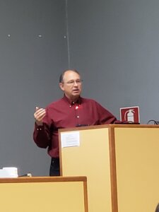
At the 8th annual INFIERI Summer School, NHanced Semiconductors president Robert Patti presented a talk on “Disaggregating System Architectures for Future HPC & Artificial Intelligence Workload” on September 9th as part of a series of invited talks at the event.
The INFIERI Summer School program includes expert lectures, keynote talks, and hands-on laboratory sessions, where participants work closely with leading scientists and industry professionals. The in-person format facilitates meaningful interactions and collaborations, ensuring a rich educational experience.
“I really enjoy discussing the next generation of semiconductors with the rising generation of high-tech specialists,” said Patti. “These international students are curious, focused, and excited about the future.”
A summary of Patti’s presentation follows:
The beginning of advanced packaging
Patti’s experience in advanced packaging technology dates to 1988 when an NHanced predecessor company sought to improve the performance of a CMOS 1.2µ dual-metal device with approximately 2 million transistors and a 325MHz FF toggle rate. They replaced the silicon CMOS with an 0.8µ GaAs device that provided a 10x higher FF toggle rate (>2GHz) but quickly discovered that it did not outperform the CMOS device even though the transistors themselves were faster. This was due to the increased wire length of the on-chip interconnects, which induced significant signal delays and power usage.
This revelation ultimately led to the conclusion that Moore’s Law (as posited by Intel’s Gordon Moore in the 1960s), predicting the industry could continue to shrink transistors and put more of them on a chip for lower cost, would eventually reach a point of diminishing returns in terms of cost per transistor. That point was reached at the 28nm node, when single-pattern lithography reached its limits, and the requirement for double-patterning and/or EUV lithography pushed manufacturing costs higher, effectively ending the transistor economics of Moore’s Law.
Paradigm shift in semiconductor manufacturing
The current semiconductor manufacturing business model – Foundry 1.0 – has been focused for the past 50 years on driving smaller transistors on more densely-packed chips. But it now faces higher development costs, higher capital costs, long development times, expensive design tools, and high risk. A sea change in this manufacturing model is underway as the industry looks to advanced packaging to deliver better cost, performance, and SWaP parameters.

Enter Foundry 2.0, a new paradigm for the semiconductor industry. Foundry 2.0 uses the chips from traditional foundries and employs advanced packaging and additive manufacturing techniques to create highly customized components and assemblies with superior performance. This new business model facilitates an expansion of the advanced packaging ecosystem, heterogeneously integrating chiplets in 3D and 2.5D to produce innovative electronic designs.
By focusing on system solutions using best of class components, Foundry 2.0 delivers lower development costs, lower capital costs, shorter development times, inexpensive design tools, and much lower risk. NHanced Semiconductors is the industry’s first pure-play advanced packaging foundry to employ the revolutionary Foundry 2.0 business model.
Advanced packaging is not a single technology
Multiple processes can be employed separately or combined to provide these performance and cost benefits, including:
- Heterogeneous integration of mixed materials in wafer-to-wafer or die-to-wafer assemblies
- Low temperature hybrid bonding (DBI®) to achieve precision stacking
- Silicon interposers: next-generation circuit boards with up to eight wiring layers
- Chiplets that enable IP reuse, lower risk, and lower costs
- 2.5D and 3D assemblies that enable system densification with reduced wire length, reduced system power, and overall lower system costs
- MEMS technologies and micro-connections for 3D structures
- Microfluidics for chip scale cooling of ultra-dense electronics
Foundry 2.0 represents a fundamental change in perspective for the industry
The next generation of semiconductors will be developed through advanced packaging, additive manufacturing, and true heterogeneous integration to achieve better ROI, lower development costs, and reduced capital expenditures. This new business model creates a system-level Moore’s Law that is based on the overall costs of next generation devices.