


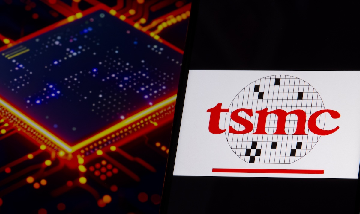
TSMC Advanced Packaging in US Scheduled for 2028; Focusing on SoIC/CoPoS
From Taiwan we hear that TSMC has accelerated Fab construction in Arizona. The third wafer fab in the United States will use N2 (2nm) and A16 process technology. It has been reported that equipment manufacturers were notified of this the second quarter of this year (2025).
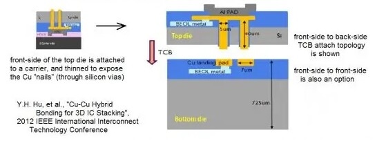
Reportedly TSMC’s two advanced packaging factories planned in the United States will be connected to the third wafer factory, and the goal is to start construction in 2028, planning to expand the most advanced silicon on integrated circuit (SoIC) and chip-on-panel-on-substrate (CoPoS) to meet the needs of local production of AI and HPC chip packaging. SoIC (known in the industry as hybrid bonding) is currently the most advanced packaging technology that TSMC has mass-produced, and will be integrated with the back-end CoWoS and even the future CoPoS (Figure 1)
Both the third fab and the 4th fab will use N2 and A16 process technology, while the fifth and sixth fabs will use more advanced technology. The construction and volume production plans of these fabs will be based on customer demand, with plans to build two new advanced packaging facilities in Arizona and an R&D center to complete the AI supply chain.
TSMC CoPoS technology is just beginning. Because the maturity of SoIC is higher than that of CoPoS, customers including AMD, Apple, Nvidia, Broadcom, etc. will be using it in high-end products first, so the current TSMC plan will be to develop SoIC in the United States first, and then introduce CoPoS later, mainly locking in the demand after 2030.
TSMC is expected to set up its first CoPoS experimental line in 2026 in Caiyu Taiwan, with mass production later in Chiayi, aiming to achieve large-scale mass production in 2028. TSMC says it feels that 2028~2029, will be the best time to introduce it in the USA.
According to industry insiders, in Taiwan, AP7 will become an important production center for advanced packaging technology, with SoIC, CoPoS and other technology production located there. In the future, the packaging type of HPC chips below 2nm will use SoIC with CoWoS, CoPoS, and InFo technologies (for example, AMD has adopted SoIC+CoWoS).
Intel Stops Glass Core Substrate Program
Intel has officially stopped funding its in-house glass substrate development, opting instead to “…source ready-made solutions from specialized vendors”.
This strategic shift is part of a broader corporate overhaul under CEO Lip-Bu Tan, focusing on core areas such as CPUs and manufacturing. The decision to abandon the glass substrate technology development is seen as a move to mitigate financial risks, and concentrate resources on core lines. Intel finances are causing it to become “leaner”, in this case, the company plans to use the growing network of glass substrate suppliers to support its glass based advanced packaging roadmap and accelerate product rollouts.
CEO, Lip-Bu Tan, has already declared that decisions will be made that involve a lot of restructuring and changes to the original roadmap. When you look at Intel’s Foundry division, it is clear that they haven’t met expectations when it comes to delivering processes to external partners, and the company’s 18A node has been a victim of delays and inconsistencies, which is why Intel is considering limiting activity around its semiconductor business. Now, the firm will reportedly use an external vendor for glass substrates, abandoning its in-house efforts.
Intel wants to reduce its operating costs and focus on core businesses, like CPU and manufacturing. Given that the market opens up opportunities for glass substrates, Intel would likely opt for external sourcing, indicating that the firm is determined to trim down its operations by cancelling projects that aren’t considered worthwhile.
Intel claims that by outsourcing glass substrates, they can “…reduce development timelines and mitigate the financial risk associated with pioneering novel substrate manufacturing”. While this may be true, IFTLE never saw Intel as a manufacturer of glass interposers, but rather assumed that their plan, all along, was to confirm efficacy and then transfer the process to trusted suppliers (who in the past have been in Asia).

This model does allow Intel the freedom to evaluate multiple suppliers, pivot quickly if performance or cost benchmarks change, and integrate advanced packaging more rapidly than if it continued to develop substrates internally. Intel hasn’t yet named which suppliers it will partner with.
Focusing on 14A and 18A-node chip production and abandoning in-house glass substrate development certainly appears to be a step in the right direction. [link].
SK Hynix, in partnership with Applied Materials, has built and is running its Absolics pilot line in Ga for a few years, while Samsung has recently scaled up its efforts in this area.
JNTC (Korea) opened its first glass‑substrate plant in May, announcing sixteen prospective clients and projecting revenues to climb from $14.7 million this year to $147 million in 2026, and ultimately hitting $735 million by 2028. A complementary facility under construction in Vietnam will triple the original plant’s output, targeting a combined annual production of roughly 500,000 substrates.
There are also Intel insider rumors indicating that “Intel has ended the Internal research and development of glass core and is NOT doing “project Management” with glass substrate suppliers”. These rumors indicate that internal focus at Intel is now on EMIB-T where the embedded bridge die has a TSV “
For all the latest on Advanced Packaging stay linked to IFTLE………………………


