

In a recent presentation by Korea Advanced Institute of Science & Technology (KAIST), and the Terabyte Interconnection and Package Laboratory (TERALAB), the firms outlined an expected HBM roadmap and detailed what they expect from the next-generation standards. The report details on the specs and performance expectations for HBM4, HBM5, HBM6, HBM7, and HBM8.
HBM4 will be the standard for next-gen data centers and AI GPUs that are launching in 2026. Both AMD and NVIDIA have confirmed the use of HBM for their MI400 and Rubin offerings. NVIDIA’s Rubin and Rubin Ultra, which will leverage HBM4 and HBM4e memory, respectively. In their roadmap NVIDIA shows Rubin with 8 HBM4 sites and Rubin Ultra with 16 HBM4 sites. There are two GPU die cross-sections for each variant, but the Ultra has the larger cross-section, forming double the compute density of the standard Rubin option (Figure 1).
Key features of the HBM generations are shown in Figure 2.
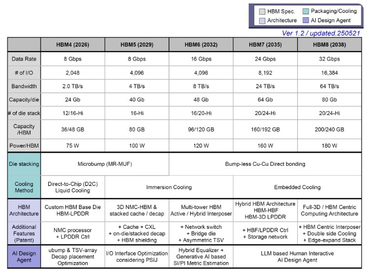
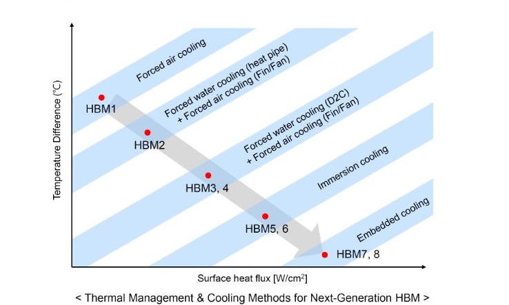
Figure 3 shows their expectations for cooling requirements for these stacked memory generations.
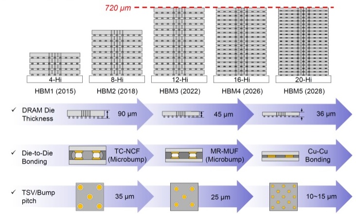
Packaging options are shown in Figure 4 with overall total thickness of the stacks topping out at 720 ums (around the thickness of a 300mm wafer)
Key features of the HBM4 memory include:
- Data Rate: ~ 8 Gbps
- Number of I/Os: 2048 (4096)
- Bandwidth: 2.0 TB/s
- Number of die stacks: 12/16-Hi
- Capacity per die: 24 Gb
- Package Power per HBM: 75W
- Packaging Method: Microbump (MR-MUF)
- Cooling Method: Direct-To-Chip (D2C) Liquid Cooling
NVIDIA’s Rubin and Rubin Ultra, are expected to leverage HBM4 and HBM4e memory, respectively. In the official roadmap, NVIDIA shows Rubin with 8 HBM4 sites and Rubin Ultra with 16 HBM4 sites.

Key features of HBM5 include:
- Data Rate: 8 Gbps
- Number of I/Os: 4096
- Bandwidth: 4.0 TB/s
- Number of die stacks: 16
- Capacity per die: 40 Gb
- Pkg Power per HBM: 120W
- Packaging Tech: microbumps
- Cooling Method: Immersion Cooling & Thermal vias
NVIDIA’s Feynman is expected to be the first GPU to utilize the HBM5 memory standard. While NVIDIA has listed a 2028 release date, this KAIST study lists what is probably a more realistic 2029 launch date for this HBM5 solution.
Key features of HBM6 memory include:
- Data Rate: 16 Gbps
- Number of I/Os: 4096
- Bandwidth: 8.0 TB/s
- Number of die stacks: 16/20-Hi
- Capacity per die: 48 Gb
- Pkg Power per HBM: 120W
- Packaging Tech: Cu-Cu Direct Bonding
- Cooling Method: Immersion Cooling
With HBM6 being the highlight at the start of the next decade, HBM7 and HBM8 will take things to a whole new level. HBM7 will offer 24 Gbps pin speeds per stack and 8192 IO lanes, double that of HBM6. The increased data rate and I/O capability will drive up the bandwidth to 24 TB/s, 3x of HBM6, and with 64 Gb capacity per DRAM die, you will see up to 160-192 GB capacity per stack, thanks to 20-24-Hi memory stacks. Each stack will have a package power of 160W. Cooling is expected to be embedded.
For all the latest on Advanced Packaging stay linked to IFTLE (Insights From the Leading Edge) ………


