At Semicon Japan, Rapidus underscored its bold decision to take on the challenge of producing 600mm × 600mm large-format RDL panels by leveraging display manufacturing technologies. Rapidus is developing 600-mm square ultra high-density interconnect panel-level packaging as an industry-leading carrier-substrate format for panel level parallel processing of multiple packages, aiming for interposer manufacturing with high throughput, lower cost and high reliability.
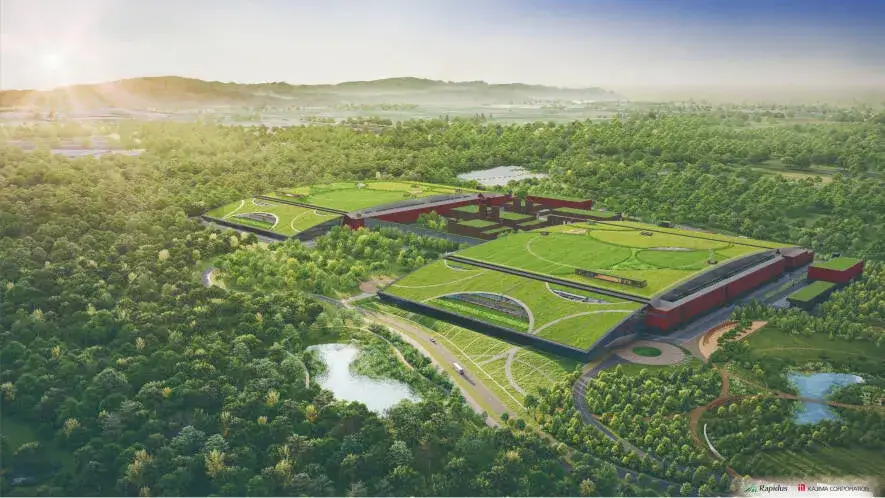
To support its packaging initiatives, Rapidus is building a cleanroom at the Seiko Epson Chitose facility in Chitose City, Hokkaido, and launched a back-end R&D hub called Rapidus Chiplet Solutions (RCS). There, Rapidus will enable 2-nm-generation semiconductor chiplet package design and manufacturing technology development, including mass-production technologies for chiplet packaging with automation. RCS will install pilot lines supporting flip-chip ball grid array (FCBGA), Si interposer, RDL and hybrid bonding processes, in addition to conducting R&D on mass-production methods including equipment automation
The mission is clear: Rapidus is redefining what Japanese manufacturing can achieve on a global stage.
For more info: Website