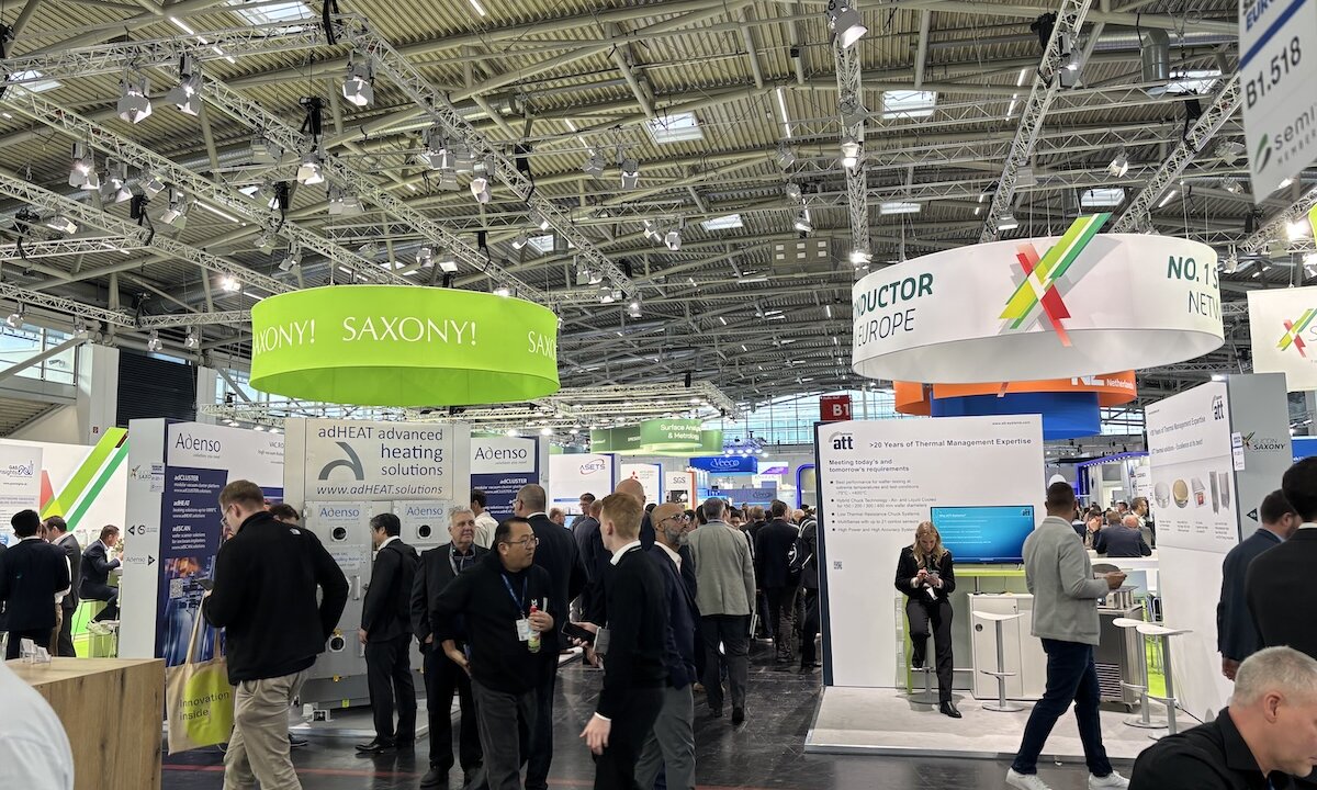
I recently attended SEMICON Europa in Germany to learn how the EU is approaching the next phase of its semiconductor development. From what I learned, the EU is moving its industry forward by planning for its CHIPS Act 2.0 legislation, attracting new investments, and funding competitive R&D pilot programs.
In addition, changing geopolitical conditions are also motivating the EU to bring more manufacturing capabilities to its member states. With mounting trade tensions between the U.S. and China, Romain Fraux from Yole Group highlighted the growing importance of supplier nationality during his November 19 keynote.
Ajit Manocha, President of SEMI, also noted that issues in the U.S. are giving Europe a chance to gain leadership. “There’s an opportunity for growth for everyone,” he said.
Europe’s Challenges and Opportunities
The EU has an ambitious goal of reaching 20% market share across the total semiconductor industry by 2030. While the 2023 CHIPS Act was enacted to help get the EU closer to this figure, many industry leaders think this could be unrealistic. Right now, the EU owns roughly 10% of the global market, and it faces a number of challenges.
On the packaging side for example, Europe’s 8% packaging market share has mainly been driven by its automotive industry. However, competition from Chinese auto makers, regional cost disadvantages, and global trade issues have strained this core pillar of its economic growth.
Second, the EU is lacking an advanced logic manufacturing facility that can produce nodes under 5 nm. Because advanced logic chips are crucial for AI, this puts the EU at a disadvantage in one of the industry’s biggest areas. AI currently accounts for about 20% of the global semiconductor market, and it only continues to grow. It’s growing so quickly that by 2030, AI alone is projected to be a $1 trillion (USD) market on its own. Although Europe lags in AI, the EU is currently working to generate investments for new factories.
However, establishing new facilities comes with the hurdle of heavy bureaucratic requirements. Because of this, several speakers at this year’s SEMICON Europa cited the urgent need to balance regulatory standards with the ability to build and innovate. For instance, Herbert Blaschitz from Exyte noted in his November 18 discussion that EU-required paperwork is expanding, which makes facility permitting and design take significantly longer than it does in Asia.
Despite hurdles, the EU also has key industry advantages that other nations lack, including world leadership in sustainability, a renowned education system that produces top talent, excellence in compound semiconductors and photonics, and its expertise in legacy technologies. The region is also gearing up for its CHIPS Act 2.0 legislation that will further bolster its competitiveness. While the exact priorities for CHIPS Act 2.0 have yet to be determined, Pierre Chastanet from the European Commission noted general interest in strengthening public-private cooperation, securing critical technologies and infrastructure, and aligning funding with strategy.
Furthermore, Chastanet also mentioned that while the first iteration of the EU CHIPS Act emphasized its response to the COVID-19 global chip shortage, the second version will focus more heavily on attracting the right investments.
Investment Successes and Pilot Programs
Although we won’t see a first draft of CHIPS Act 2.0 until early next year, the EU has secured several prominent investments on the front-end. The European Semiconductor Manufacturing Company (ESMC), in partnership with TSMC, Robert Bosch GmbH, Infineon Technologies AG and NXP Semiconductor, is building what will soon become “the EU’s first FinFET-capable pure-play foundry” in Dresden, Germany.

Once completed, the facility will have a production capacity of 40,000 300mm wafers on TSMC’s 28/22 nm planar CMOS and 16/12 nm FinFET process technology, as reported in an NXP press release. Total investments are projected to be more than 10 billion euros.
Another big investment win is STMicroelectronics’ 5 billion euro investment in Catania, Sicily for a new silicon carbide plant. This comes in addition to the company’s 60 million euro investment in Tours, France that will support a pilot line for advanced semiconductor manufacturing technology. Since the first EU CHIPS Act was introduced in 2023, the EU has now secured more than 1 billion euros in combined public and private investment.
A crucial aspect of CHIPS Act 1.0 was its funding of several R&D pilot programs – another area of EU leadership. These pilot programs aim to close the gap between research and production by speeding up developments and focusing on scaling. For instance, Fraunhofer-Gesellschaft is leading the Advanced Packaging and Heterogeneous Integration for Electronic Components and Systems (APECS) program to accelerate chiplet innovation. This is important, because newer packaging architectures like chiplets are becoming increasingly essential for improving upon AI.
Final Thoughts
It’s no secret that the global semiconductor industry is undergoing a transformation. As regions around the world prioritize supply chain localization and settle into core areas of expertise, I think the EU can excel, so long as it sticks to a unified plan. This is where CHIPS Act 2.0 will come into play.
Although it’s too soon to tell which efforts the updated legislation will prioritize, the direction for the future of the European industry seems like it’s still up for debate. Based on the sessions I attended, there seemed to be a notable divide between those who want to allocate more funding to the EU’s existing areas of expertise, and those who want to direct new funds toward lesser-developed sectors like AI. While one side states that there’s no point in trying to catch up to the U.S. or Asia in AI, the other side believes that the EU will never reach its 20% market share goal without attempting to succeed in this area.
My gut instinct is to agree with the latter argument, but nevertheless, I think the EU CHIPS Act 2.0 will be pivotal for Europe’s industry.