
Adeia vs AMD
Hybrid bonding is a semiconductor packaging technique that enables direct Cu-Cu and oxide-to-oxide connections, eliminating the connection using microbumps. This approach improves interconnect density, electrical performance, and thermal efficiency, making it an important advanced packaging technology for next-generation semiconductor devices.
Adeia Semiconductor Solutions, a wholly owned subsidiary of Adeia Inc ( formerly Xperi, formerly Invensas, formerly Tessera) has filed a pair of patent infringement lawsuits against AMD in the U.S. District Court for the Western District of Texas, claiming that AMD’s chips incorporate patented innovations covered by its hybrid bonding IP portfolio.
Evidently ten patents are at issue — seven covering hybrid bonding and three tied to process nodes used in advanced logic and memory manufacturing. Asserted patents in the first case include: 8,389,378, 10,879,226, 12,401,010, 9,564,446, 11,978,639, 10,283,592. Asserted patents in the second case include 11,978,681, 12,199,069, 12,322,650 and 12,381,173.
Adeia claims that the litigation, announced November 3, followed what Adeia describes as years of failed licensing talks. AMD has not yet commented. Adeia says AMD’s products make “extensive use” of the same concepts, asserting that its patented work has “greatly contributed” to AMD’s success.
AMD’s roadmap leans heavily on stacked designs, not just for Ryzen but for EPYC and future accelerators that layer compute, memory, and I/O.
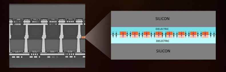
Hybrid bonding technology (direct Cu-Cu bonding tech) is used in AMD’s 3D V-Cache design. Instead of solder bumps, allowing a 64MB slab of SRAM to be stacked on each compute die. The technique is known to use TSMC’s SoIC process.
Adeia, which spun out of Xperi, claims ownership of a large portfolio of bonding and interconnect IP.
Beginning ~ 2000, Ziptronix pioneered the development of innovative low-temperature bonding techniques for semiconductor chips. Ziptronix developed ZiBond, a direct bonding technology, and Direct Bond Interconnect (DBI), a hybrid bonding technology. Lead innovators at Ziptronix included Qin-Yi Tong, Gill Fountain and Paul Enquist who are recognized as the earliest inventors of direct and hybrid bonding. Tong and Enquist are both deceased.
In 2015 Tessera acquired Ziptronix, Inc. for $39 MM.
Its DBI and ZiBond technologies have since been licensed to major players in memory, CMOS image sensors, and 3D NAND.

Few experts expect any near-term disruption to AMD’s products, since injunctions in patent cases of this kind are rarely granted. The question is whether Adeia’s claims can survive the early procedural hurdles that often decide the outcome long before trial.
AMD and its foundry partners are almost certain to challenge the patents through inter partes review at the Patent Trial and Appeal Board, arguing that the asserted claims are either too broad or already covered by TSMC’s process IP.
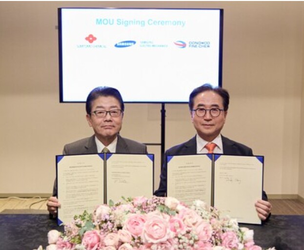
Samsung EM MOU with Sumitomo Chemical
Samsung EM (Electro-Mechanics) announced that it has signed a memorandum of understanding (MOU) with Sumitomo Chemical Group to establish a joint venture (JV) for manufacturing ‘Glass Core,’ a key material for next-generation package substrates.
The joint venture MOU is part of a strategy to overcome the limitations of current package substrate technology for artificial intelligence (AI) and high-performance computing (HPC). ‘Glass Core’ is claimed by some to be the natural, next-generation semiconductor package material, thanks to its lower coefficient of thermal expansion and superior flatness compared to conventional organic substrates.
In the joint venture, Samsung Electro-Mechanics will serve as the primary investor, while Sumitomo Chemical will participate as a minority shareholder. The companies plan to finalize a corporate name, and aim to sign the main agreement next year. The headquarters will be located at Dongwoo Fine-Chem’s Pyeongtaek site, which will also serve as the initial production base for ‘Glass Core’.
Samsung Electro-Mechanics is currently producing glass package substrate prototypes at its Sejong plant pilot line. Mass production is planned to begin with the joint venture after 2027.
For all the latest in advanced packaging stay linked to IFTLE……………………..