This Fall has been a busy time for semiconductor events. Starting with SEMICON Taiwan at the start of the month, IMAPS in Late September into early October, followed closely by SEMICON West last week. Fortunately, there is a month off to catch your breath before heading to Semicon Europa.
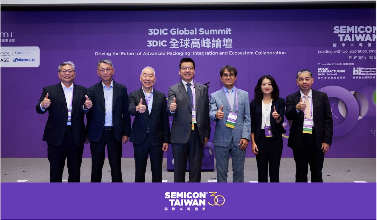
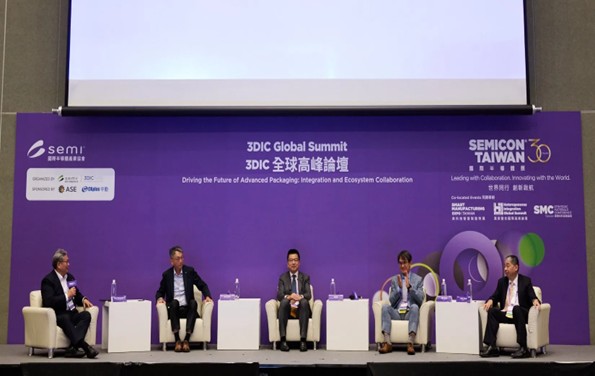
There has been a series of packaging announcements, starting with Semicon Taiwan, that warrant highlighting. At Semicon Taiwan, SEMI announced the launch of the 3DIC Advanced Manufacturing Alliance (3DICAMA).
TSMC and long-time partner ASE will co-chair the effort with Dr. Jun He, Vice President of Advanced Packaging Technology and Service at TSMC, and Dr. Mike Hung, Senior Vice President at ASE, acting as the joint co-chairs. 37 different companies have signed up to participate. Those mentioned specifically at the conference, and in the press release, are All Ring, Chroma, Delta, Everlight Chemical, GMM, Grand Process, Scientech, and Unimicron.
Other companies thought to be participating are: Nvidia, Sony, Broadcom, AMD, Sunlight, Lam Research, Lightmatter, MediaTek, Innolux, PDF solutions, Power Tech technology and Utechzone. Since that’s only 20, there are several more who will participate and help to develop the 3DIC ecosystem.
3DICAMA has several lofty goals, such as creating a resilient ecosystem, setting standards, and looking at how to develop and improve the 3D packaging process to make it into a manufacturable industry-wide technology. Other key issues are looking at how to address the thermal issues and interconnect challenges. The kickoff of the alliance featured a summit to discuss some of the burning issues facing the advanced packaging industry and look at how collaboration might help to speed the development of a complete and sustainable 3DIC solution.’
It will be interesting to see how open or closed this alliance becomes. The initial group is very Taiwan-focused, which shouldn’t be a surprise, as TSMC and ASE are two of the product leaders in the 3DIC space. As a result, many of the Taiwan suppliers are already heavily invested in the Taiwan 3D packaging space. Also, will they use the UCIe standards that have been developed and build upon those, or are we entering a brave new world?
Participants in the 3DIC space are aware of how complicated integrating all the pieces into the multi-reticle packages and the key role that interposers will play in creating a stable package. Polymers, silicon, and glass are all candidates, but as always in the semiconductor industry, there is a difference of opinion as to what will work best.
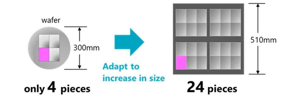
Resonac announced during the week of Semicon Taiwan a consortium that will be focused on creating polymer interposers on a 515 mm x 510 mm panel. The project called Joint 3 will have 27 members, many of them already participate in other Resonac packaging projects. The objective is to create polymer interposers using panels rather than wafers. There is a significant advantage in the area, enabling more interposers to be created, helping to reduce costs, and increasing the size of the packages.
Meanwhile, Trendforce reported that Apple and Tesla are considering replacing silicon and organic interposers with glass interposers. Glass is cheap, can be processed easily (Think flat-panel displays), and it can reduce warpage or post-process flow that can happen with organic interposers. There are some process challenges with glass, as it can crack when drilling deep vias or dicing up into smaller pieces.

Multiple manufacturers besides Tesla and Apple have been exploring glass substrates, including Intel, TSMC, and Samsung, just to name three of the leaders in 3D packaging, so there is a considerable effort in the space. In addition, the panel industry is experienced in handling and cutting glass. This has the potential to accelerate glass as the interposer for larger panels if the technical challenges can be worked out, and it proves to be as effective as polymer technology.
At the end of September, TSMC began its Open Innovation Platform tour. The event allows TSMC to showcase its progress and roadmaps for next-generation transistor technology, advanced packaging, as well as TSMC’s partnerships that enable it to be the most effective foundry in the world.
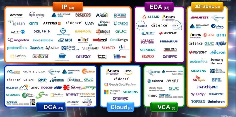
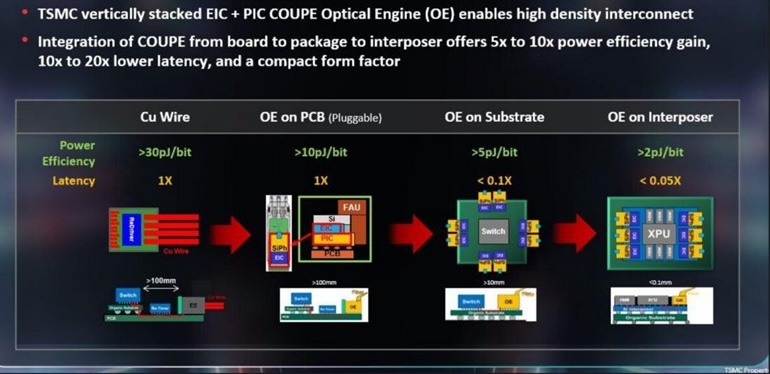
One of the key points at the OIP presentation was that the EDA companies all have software developed that enables companies to design 3D systems compatible with the TSMC CoWoS process and 3D Fabric technology. This eases TSMC’s customers’ design path to 3D technology. What is also important about design advances is that photonic design is also included, which will improve data transfer from the system to the outside world. The photonics technology also has the potential to reduce power consumption, which is sorely needed.
Advances in TSMC’s 3D Fabric are also helping to improve performance. The move to 12 high HBM 4 will improve memory data transfer by improving bandwidth and efficiency. Micro bumps are shrinking from 0.45um to 0.25um, which allows for scaling and more IO where needed. The Co-packaging of optics has proven to increase the efficiency of data transfer, reducing latency and improving system efficiency.
The advances will help TSMC’s customers put more features in the system packages and enable them to operate at improved power efficiency. While it won’t solve the power problem that data centers are creating. It will assist in creating more efficient AI systems.
The ecosystem partnerships and consortia that are being built around the advanced packing space demonstrate the critical nature of its needed success. The complexity of the systems needed for advanced computing for data centers, as well as computing on the edge, is driving the system in a package to new heights. While in some cases disintegration is happening, the result seems to be more efficient systems, which can have lower latency due to integrated photonics and potentially use less power, or process more data with the same levels of power. The consortia will help to reduce time to market, and hopefully create leading-edge standards to improve system performance.