Rejects can occur at various stages of semiconductor processing. The further downstream a reject occurs, the more costly the defect as each processing steps consumes more time and resources. The worst possible failures occur after the device has left packaging and assembled into a final product. Such failures can lead to catastrophic failures including the loss of life.
Most rejects are captured at wafer or final assembly test. Unfortunately some rejects will only occur under subsequent processing or during operation in the final product. Assembled units with unknown defects are termed “walking wounded” units. These walking wounded can kill the reputation of even the most respected supplier. It’s imperative to identify failures to feedback into the manufacturing operations for improvement but more importantly to assure now such devices can continue along the assembly path ending up in a product where loss of life could occur.
Failure analysis helps to isolate and identify where the problem has occurred, implement improvement and track to assure the culprit has truly been identified. Yet failure analysis can lead one down a dark path of hours of investigative work, and at times leading to incorrect assignable root cause(s). If inexperienced investigators use the wrong analytical tools and hard de-processing processes, the true root cause may be removed, placing fault incorrectly.
Take, for example. The delamination in an overmolded package. Typically deprocessing methods would involve using aggressive acids, lasers, plasmas and polishing. All of these can blow right past a possible root cause during overmolded decapsulation of the package.
Lasers vaporize everything. Acids are not precise, can dissolve the root cause, are extremely dangerous, present disposal issues, and can damage the die, thus eliminating the chance for electrical validation.
Plasma is slow and requires multiple plasma gas types to remove subsequent layers of organic, inorganic and some bio solutions. Some of these gases also eliminate, react and modify the root cause unknowingly. Plasma decap is also very slow.
Polishing is fast but if it lasts a second too long, the wrong grit is used or has poor planarity, the layer is destroyed. Polishing is also dirty, and likely introduces artifacts that can be mistaken as in-situ particles.
A friendlier investigative tool preserves all possible artifacts that could be the true root cause.
Failure Analysis Case Study
A customer had a problem with delamination in plastic packaging. One prior F/A result was inconclusive after months of evaluation. A second using lasers and acids likely blew right past what my team suggests could be the true root cause.

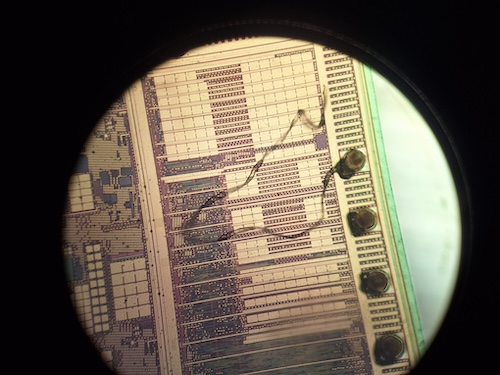
This kinder and gentler approach uses a custom blended solvent. The solvent effectively breaks the bond between the die and the mold compound allowing for a perfect release. As a result, we were able to spot a fiber attached near one of the wirebonds.
At first observation, the assumption was the fiber was an artifact of our processing. But after optical inspection of the top of the mold compound, a clear imprint of the fiber could be seen in the mold compound corresponding to the exact location on the die. A reverse image of the die and fiber is clearly visible suggesting that the fiber likely created a time zero air (delamination) gap from the space and decomposition products during mold
Depending upon the makeup of the fiber, further heating likely exacerbated the problem with additional decomposition and expansion of trapped air and gasses. Figure 1 shows the fiber in the upper quadrant attached to a wirebond post. This fiber could have occurred at wire bond, during transport to mold or at molding itself. Regardless it’s a backend assembly issue that needs to be addressed.
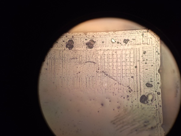
Figure 2 shows the interior to the mold compound with the impression of the wire. Missing is the mirror image of the die contour in the location of the fiber providing further evidence of the placement prior to decap. Missing imprints of the die also suggest the die was outgassing during molding as the surface contour of the die is blurred and distorted in the area where the fiber was located.
While it’s possible this fiber might not be the true root cause, experience suggests investigating the overmold areas for cleanliness. Fibers can have any number of sources but an analysis of the fiber using FTIR might lead to the direct source suggesting the proper controls to reduce real time and walking wounded failures.
In additional to wirebonded overmolded packages, the approach lends itself to BGA and uBGA molded packages as well. The extraction process also allows reuse of extract die for repackaging with much better results than traditional deprocessing techniques and at less the cost.