
By Till Dreier & Julius Hållstedt
Non-destructive X-ray inspection has become a critical capability across the semiconductor and electronics industry — from ramp-up phases to high-volume production and failure analysis. In production, both automated X-ray inspection (AXI) and manual (MXI) at-line inspection are essential for maintaining process control, ensuring quality, and detecting defects as early as possible. Also, during failure analysis, non-destructive methods are often preferred to preserve a device’s integrity so that it can still be electrically tested after imaging. As in many cases, it is necessary to utilize several different complimentary methods in order to be able to fully understand root causes and failure mechanisms.
Generally in AXI, non-destructive testing typically relies on 2D images. Today’s advanced packaging and interconnect technologies consist of many chips and structures connected on top of each other. This means that traditional 2D AXI can miss subtle or defects hidden behind other features. This is illustrated by the 2D projection image example in figure 1. It is evident that the increasing complexity of structures in modern advanced packaging demands 3D information in order to reliably identify defects from the full volume.

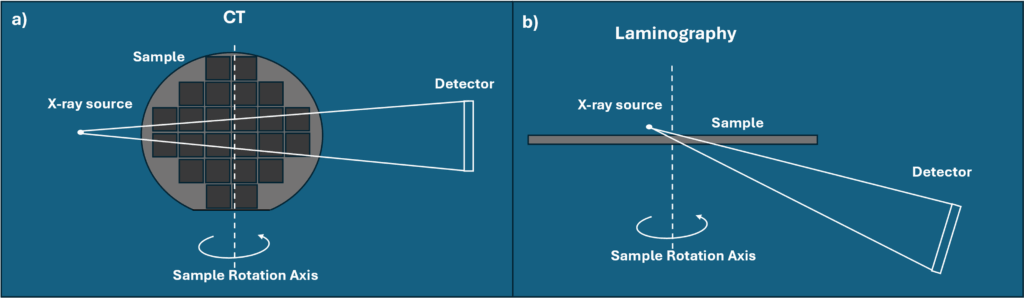
Many semiconductor and electronic components — such as wafers, chip packages, and printed circuit boards (PCBs) — are inherently large but at the same time flat and thin. This geometry poses a challenge for conventional computed tomography (CT), which requires the sample to be rotated within the X-ray beam as illustrated in figure 2a. Besides being impractical, it forces the sample to be put relatively far away from the X-ray source, limiting magnification and reducing measurement speed as intensity is reduced by the inverse square law as described in our previous article [1]. Consequently, this typically results in the need for destructive sample preparation reducing the sample size to achieve high resolution nano-CT as described in reference [2].
Laminography and related techniques such as planar CT and tomosynthesis provide a powerful alternative as was first proposed in 1974 [3] and later implemented in conventional X-ray projection imaging in 2005 [4]. In laminography, by using a planar rotation of the sample and positioning the detector at an angle, as illustrated in figure 2b, high resolution imaging of planar devices can be obtained efficiently. This makes the technique well suited for non-destructive inspection of large, flat samples common in semiconductor and electronics manufacturing, as the sample can be put close to the source and thereby enabling largest magnification, greatest intensity and highest measurement throughput. An important fact to remember is that the geometry is based on cone beam geometric magnification where the X-ray source spot size is just as important as in nano-CT and stability of the system is crucial, see the previous articles [1, 2] for more details. The spot size and shape are thus directly affecting the resolution and therefore careful optimization of X-ray source spot size should be performed to achieve the right resolution with highest throughput. Systems enabling highest resolution laminography often rotate the detector instead of the sample to avoid magnifying errors of the rotation axis.
In short compared to nano-CT, which can deliver exceptional resolution but may require destructive preparation for larger samples, laminography (and related techniques) preserves the sample’s integrity while still delivering high-quality volumetric data at highest throughput.
X-ray Imaging of an HBM Stack with Laminography
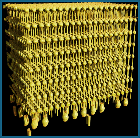
Figure 3: 3D render of eight layer HBM stack generated from the laminography measurement.
As an example, we performed measurements of a GPU wafer sample containing a stack of eight HBM DRAM modules. These are interconnected using 5 µm TSVs and 20 µm microbumps. More details on the setup used can be found in reference [5]. A 3D rendering of the region of interest (ROI) is shown in Figure 3, providing an overview of the inspected structures.
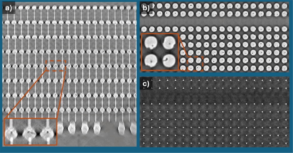
Virtual slices extracted from the reconstructed volume are illustrated in Figure 4, both in the horizontal and vertical directions.
The horizontal slice, benefiting from higher in-plane resolution, clearly reveals voids and other defects within the microbumps. The vertical slice, while affected by reconstruction artifacts associated with the missing cone of the laminography geometry, still provides valuable information on TSV alignment, as well as small defects in the microbumps. In addition, virtual slicing through the TSV array enables direct inspection of these features, allowing assessment of their continuity and uniformity.
Notably, features positioned closest to the X-ray source appear with higher effective magnification than those further away, enhancing defect visibility but requiring careful interpretation. Furthermore, as with other X-ray techniques, beam hardening – i.e. artefacts caused by highly absorbing features – can occur in laminography, potentially influencing contrast in regions close to e.g. larger bumps.

Summary and conclusion
This article highlights X-ray laminography as a powerful alternative to conventional CT for non-destructive 3D inspection of flat, large semiconductor samples such as wafers and advanced packages. Unlike CT, which requires full rotation and often destructive sample preparation, laminography uses a tilted planar rotation that keeps the sample close to the source, enabling high magnification, high throughput, and preservation of sample integrity. By designing an imaging system with a state-of-the-art nanofocus X-ray source allowing for sufficient magnification while assuring a stable system and reliable sample rotation, sub-micron laminography is achievable.
Proof-of-concept measurements on a GPU wafer with stacked HBM modules, interconnected with 5 µm TSVs, and 20 µm microbumps demonstrates laminography’s ability to detect voids, defects, and TSV alignment on sub-micron scale. Although missing-cone artifacts, magnification gradients, and beam hardening must be considered, laminography delivers high-quality volumetric data ideally suited for advanced packaging and interconnect inspection.
References
[1] T. Dreier and J. Hållstedt, “Unlocking the Mystery of X-Ray Imaging for Electronics and Semiconductor Inspection,” 3D inCites, 23 April 2025. [Online]. [Accessed Sep. 29 2025].
[2] T. Dreier and J. Hållstedt, “Revealing the Invisible: Optimized nano-CT Case Studies in Advanced Packaging” 3D inCites, July 1 2025. [Online]. Available: [Accessed Sep. 29 2025].
[3] F. A. Hasenkamp, “Radiographic Laminography”, Mater Eval 32, 169 (1974).
[4] L. Helfen, T. Baumbach, P. Mikulík, D. Kiel, P. Pernot, P. Cloetens, J. Baruchel, “High-resolution three-dimensional imaging of flat objects by synchrotron-radiation computed laminography,” Appl. Phys. Lett. 86 071915 (2005).
[5] T. Dreier, D. Nilsson and J. Hållstedt, “Fast and high-resolution X-ray nano tomography for failure analysis in advanced packaging,” Microelectronics Reliability, vol. 168, p. 115694, 2025.


