Koh Young Technology, the global leader in True 3D measurement-based metrology and inspection solutions, will make its first appearance at IMAPS 2025, the premier event for microelectronics and advanced packaging, taking place September 29 through October 2, 2025 in San Diego. The participation underscores Koh Young’s growing commitment to the advanced packaging and semiconductor industry. At booth 805, Koh Young experts will be available to discuss the proven Meister Series and the ZenStar platform, both designed to address the evolving challenges of next-generation semiconductor packaging.
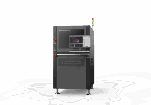
The Meister Series has established itself as a benchmark for high-resolution inspection of System-in-Package (SiP), Advanced Package, and 3D semiconductor devices. Delivering high resolution, precision optics, and AI-driven analysis, the Meister Series provides accurate measurement of critical dimensions, bumps, pillars, and other essential structures. Its versatility makes it equally valuable in R&D environments and high-volume production lines where yield and reliability are critical.
Addressing, wafer-level metrology, the ZenStar builds on Koh Young’s True 3D measurement foundation to deliver the speed, accuracy, and scalability required for the applications. As advanced device architectures push the limits of conventional metrology, The ZenStar provides semiconductor and packaging engineers with the performance and confidence needed to maintain process stability and accelerate time-to-market.
“Our first appearance at IMAPS reflects Koh Young’s focus on advanced packaging and semiconductors,” said Allen Phung, Head of Sales for the Americas at Koh Young America. “By combining the proven performance of the Meister with the scalability of the ZenStar, we’re helping manufacturers achieve higher yield, greater reliability, and faster time-to-market for next-generation devices.”

Koh Young will be available in booth 805 throughout the event to share insights, discuss application challenges, and highlight how its solutions are shaping the future of semiconductor packaging. Attendees can also learn more by visiting www.kohyoungamerica.com.