Today’s rapid growth in 3D heterogeneous integration (3D HI) is being driven by a plethora of high-performance computing applications driving the microelectronics industry, including autonomous driving and artificial intelligence.
This strong need for 3D HI has pushed capital expenditures for advanced packaging at a remarkable pace. The advanced packaging market is projected to grow at a CAGR of 9.4% from 2024 to 2030 with a rise from more than $45B in 2024 to almost $80B by 2030, according to Yole.
These advancements required new process technology and process equipment to produce high density advanced packages with high yields. These backend devices are manufactured on 300mm wafers and require low defectivity levels that were previously restricted to front-end processes. As a result, new toolsets need to have low defectivity to obtain high yields, while delivering a low cost of ownership.
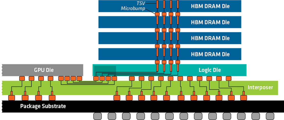
When stacking chips in a 2.5/3D package, as shown in Figure 1, several techniques can be used to interconnect the devices, including bumps, micro bumps, pillars, through-silicon vias (TSVs), and hybrid bonding. These can connect the die directly to the substrate, or to an interposer made of various materials such as glass, silicon, or organic materials. Package architectures implementing these processes include die-to-die, die-to-interposer and die-to-substrate. There are several wet processes in the Advanced Packing process flows that are required to create these bonding structures. In this article, we focus on advanced cleaning for 3D structures in high volume manufacturing (HVM) that use micro bumps to connect homogeneous dies stacks, such as high bandwidth memory (HBM) shown in Figure 1 that require similar die stack flux removal processing. We will also cover 3D HI for hybrid bonding-temporary bonding material removal, post die singulation strip, die stack flux removal and pre-bond cleans.
Solving Bump Cleaning for High Bandwidth Memory Applications
While the future of bonding high-bandwidth memory (HBM) stacks is hybrid bonding, bumping technology is still prevalent in high volume manufacturing today. The memory dies for HBM3E are stacked twelve high on top of each other with a 10µm die spacing and on a 10µm pitch. Bumping for HBMs poses significant challenges for the cleaning process.
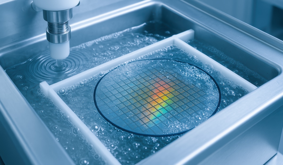
Flux cleaning is critical to wafer bumping and joint formation processes because it removes oxide layers and other impurities left by solder materials, which will impact bonding and electrical characteristics. To ensure a clean metallic interface for the next assembly step, a fluxing agent is delivered to the bumped surface. For 3D structures it is extremely challenging to remove the flux residue after the bump bonding process because the top die blocks direct spraying and gaps between die and bumps can be only 10 µm.
Soak-and-spray technology enables the cleaning platform to remove flux residues down to the 10 µm spacing. The wafers are first immersed in the appropriate chemistry to dissolve the flux material. The head of fluid forces the chemistry throughout the open spaces in the die stack. The wafer is then then transferred wet to the high-pressure spray chamber, where the spray angle and high-pressure spray pressure remove any remaining flux and exchange the chemistry in and around the bumps. After undergoing the solvent high-pressure spray, the wafers are transferred again into an immersion/spin chamber sequence with rinsing fluid to displace any solvent or flux residues to prepare the wafer for spin dry. As this approach has been demonstrated to be robust and repeatable, it is currently used in high volume manufacturing for HBM3E. This technology is current being refined to meet HBM4 spacing down to 5 µm. The reduction in bump size permits the die stack to be increased to 16 high.
For larger bump geometries, such as 100 µm or 50 µm spacing, a spin-only process is possible. This process is used in AI structures mounting the HBM stack in proximity to logic, or other die either with or without an interposer. Flux cleaning at the interposer level for 2.5 D designs (or bump interface for 3D designs) for chip-on-wafer (CoW) applications can be accomplished with spin-only processing that employs high-pressure spray and low-surface tension fluids. Processing includes advanced techniques for exchanging fluid throughout the die levels and requires extremely high-speed, high acceleration and vibration free spinning of unbalanced substrates.
Cleaning Technologies for 3D HI
As 2.5 and 3D HI packages continue to evolve, dimensions will shrink below 5 µm, eventually necessitating a transition from bump bonding to hybrid bonding for improved packaging efficiencies. The tight tolerances needed to achieve 3D HI devices creates unique challenges for the cleaning process. As device dimensions shrink, it’s critical to create clean surfaces both for the deposition of materials and to facilitate material bonding. When connecting 100 µm bumps, small defects in the 200 nm range do not impact yield. Any contamination can impact the electrical quality of the film being deposited, as well as material adhesion, especially when dimensions shrink below one micron.
Cleaning is Critical for Hybrid Bonding
Hybrid bonding is achieved by manufacturing co-planar conductor and dielectric surfaces. These surfaces must be oxide- and residue-free to permit proper bonding, as residues on the bonding surface can make voids more than an order of magnitude larger than the defect. Critical cleaning processes for hybrid bonding include die singulation, photoresist strip, temporary bonding material removal, and pre-bond surface cleaning. One tool can handle all the various process steps that require multiple chemistries and the ability to handle wafers and wafer stacks of various thickness and warpages.
Photoresist is used as a mask for the plasma die singulation. This process leaves a plasma hardened resist on top and fluorocarbons down the sidewall of the die. Effective cleaning of the residual polymers is performed by using an immersion chemistry that begins to effectively dissolve the plasma-exposed photoresist mask and the sidewall polymer residue.

Once the majority of polymer is dissolved, the wafer is transferred while wet into a high-pressure spray chamber, where the spray pressure can be ramped and controlled up to 3,000psi. In the chamber, any remaining residues are removed, leaving clean surfaces and sidewalls. In some cases where direct line of spray is impeded, a megasonic head can be beneficial in removing debris when used in tandem with a high-pressure spray. This process sequence has proven effective in removing post plasma die singulation residues.
The die singulation process in many cases is done in two plasma steps. The wafer containing the die is attached to a carrier wafer using temporary bonding material (TBM). The first plasma step is a partial die singulation. The photoresist mask and fluorocarbon byproducts are cleaned via wet process and the wafer flipped onto a second carrier wafer that also employs a TBM. The backside silicon is then thinned via grinding, cleaned, spin coated, exposed, and developed to prepare for the second half of the plasma die singulation process. When the second plasma dicing process is complete, the photo resist mask and sidewall fluorocarbons require a second cleaning step. Final cleans to remove any residual debris for the photo resist, or any of the several TBM materials is required immediately prior to die transfer.
Figure 2 from 2023 gives the results of such a process sequence, demonstrating up to 97% yield and excellent hybrid bonding with features as small as 5µm. Recent data shows much higher yields can be obtained and hybrid bonding accomplished down to 200 nm pitch.
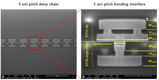
Figure 2: Using a strip and clean process for removing temporary bonding material prior to hybrid bonding resulted in up to a 97% yield for features as small as 5µm. (Source: Veeco)
Before bonding the wafer or die together, surfaces need to be particulate and oxide-free, and an activation process ensures the bonding process is successful. This can be accomplished with an oxygen atmospheric plasma in the wet process tool to remove residual organics and a second plasma in the bonding tool to remove any surface oxides.
Summary
Cleaning requirements for today’s high-density 3D HI devices are diverse. The required combination of processes and cleans necessitates a cleaning tool with significant process versatility that can ensure high yields for a multitude of processes on geometries requiring more than immersion or low-pressure dispenses alone. These processes, which include resist strip, temporary bonding materials strip (adhesive, mechanical and/or laser release), pre-bond cleaning and Chip on Wafer (CoW)/HBM die stack flux removal, can be combined on a wet processing platform to provide state-of-the-art cleaning for advanced packaging with a low cost of ownership.
A versatile multi-chamber cleaning system capable of multiple immersion chemistries, utilizing surface cleaning techniques such as high-pressure spray, high-velocity spray, and megasonics will surpass todays 3D HI cleaning requirements. Implementing such an integrated platform optimizes the advanced 3D packages needed for high-performance computing essential to burgeoning AI and other microelectronic applications.