
One form of advanced packaging is 3D stacking, in which two (or more) chips are stacked together. This differs from interposer-based packaging, in which a silicon (or other type of) interposer is used as a base to place multiple die side-by-side on the interposer. In that case, the interposer has routing to connect those die to each other as well as to the routing in the rest of the package. In a 3D stack, the stacked die have routing and processing to connect them to each other.
A true 3D process is attractive for many reasons, such as reduced area footprint, improved performance due to shorter interconnect, enhanced power efficiency, and more [1]. However, this process involves putting vias in chips, risking defects in expensive silicon. Other design considerations, such as thermal constraints, must be considered as well.
The goal of this analysis is to explore the cost drivers associated with a face-to-back chip-on-wafer 3D stacking process. Once the cost components of a complicated process like this are known, package and chip designers, material and equipment suppliers, and others can make informed decisions when using this advanced packaging technology.
Activity Based Cost Modeling
Activity based cost modeling was used to construct the chip-on-wafer 3D process flow used in this analysis. With activity-based cost modeling, a process flow is divided into a series of activities, and the total cost of each activity is calculated. The cost of each activity is determined by analyzing the following attributes: time required, amount of labor required, cost of material required (consumable and permanent), tooling cost, all capital costs, and yield loss associated with the activity.
Process Flow
The process flow used for this 3D stacking example is a face-to-back process. The name of this process describes the surfaces of the two wafers that touch: the face (top) of the incoming (top) die is in contact with the back of the bottom wafer. Though-silicon vias (TSVs) are in the bottom wafer; the bottom wafer also has backside metallization [2].
A face-to-back process can be done in a few ways. It does not have to be chip-on-wafer; if the top and bottom die will be the same size after dicing, then this process can be done as a wafer-on-wafer process. There are also multiple bonding methods. This analysis focuses on hybrid bonding, but other types of chip and wafer bonding may be used. The process flow is listed below.
Top Wafer (Top Die)
- Start with incoming wafer
- Grind to desired thickness
Remaining steps are carried on face:
- Create passivation layer
- Carry out hybrid bonding metallization
- Mount on dicing tape and dice
- Final hybrid bonding preparation
Bottom Wafer
- Start with incoming wafer
- Create TSVs
- Add redistribution layer (RDL) if needed
- Bond to carrier wafer to work on backside
- TSV reveal and thinning
- Carry out hybrid bonding metallization
- Final hybrid bonding preparation
- Carry out hybrid bond of incoming die
Final Activities
- Debond from carrier wafer
- Bond to new carrier to work on face of main wafer
- Optional RDL(s)
- C4 bumping
- Dice die-to-wafer stack into final package size
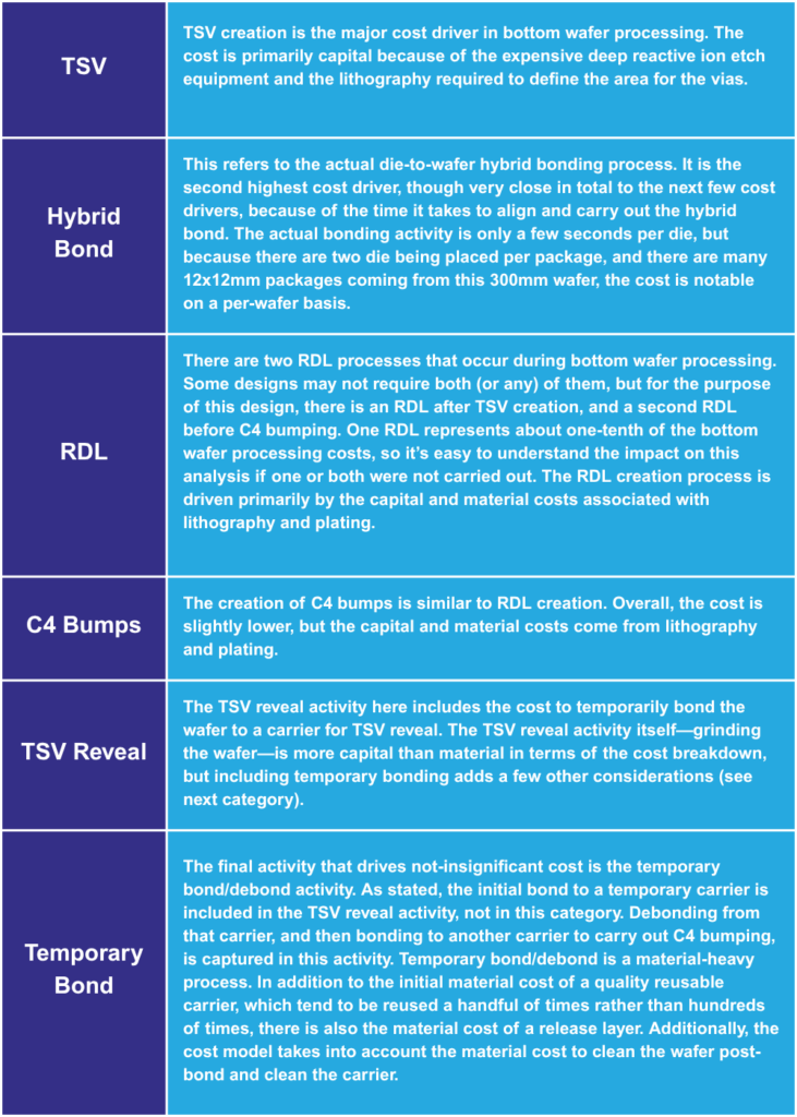
Cost Breakdown
The design used in this analysis is a 4x4mm die from a mature node placed on a bottom wafer from a more advanced node. Two die are placed per package. The final package after bonding is diced into a 12x12mm package.
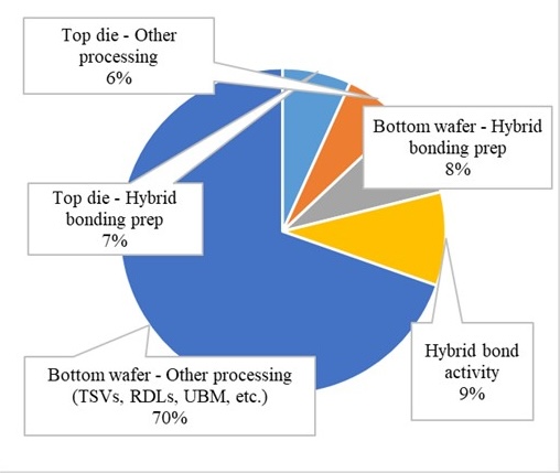
The pie chart in Fig. 1 shows the cost breakdown of all processing for both the top and bottom wafers. The cost of silicon and the cost of yield loss are not included. The cost to prepare for hybrid bonding and the cost to carry out the hybrid bond itself are separated into discrete categories.
The chart shows that processing the top die does not represent a major portion of cost in the scheme of the full package. This makes sense, as there is limited processing occurring—no TSVs, no major layers of routing, etc.on the top wafer that becomes the top die. Hybrid bonding preparation is not negligible for either the top or bottom wafer from the perspective of cost contribution, but the major cost contributors come from TSV creation and other processing of the bottom wafer.
The chart in Fig. 2 adds yield loss to the picture. Because one of the wafers is from a more advanced node, the cost of silicon in the design is more than $10,000, so even a small yield loss can move the needle.
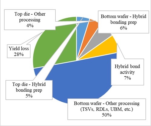
Figure 2. Face-to-Back Package – With Yield Loss
The next section of analysis further breaks down the cost of processing associated with the top and bottom wafers.
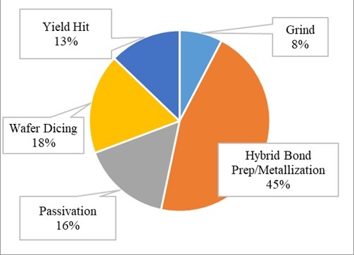
The major cost driver associated with top wafer/die preparation is the metallization for the hybrid bonding process (Fig. 3).
Dicing the wafer is the second higher cost driver. Dicing is not a complicated or new process, but because this is a small (4x4mm) die, the dicing process shows up as a notable piece of the pie. The larger the die, the smaller the total dicing cost when using a linear-based process; in this case, laser scribe and saw is the dicing method modeled.

The cost to add a passivation layer prior to hybrid bond metallization is the third highest cost driver. This process involves lithography steps, which carry both capital and material costs.
The next chart breaks down the cost of bottom wafer processing (which also includes the steps captured in the final activities segment above: after the top die has been bonded, the package must be completed with C4 bumps, optional routing, etc.).
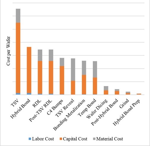
In contrast to the top wafer/die cost breakdown, which showed the contribution of only five activities, there are many more activities carried out as part of bottom wafer processing. The chart in Fig 4. not only shows the comparative cost of these different activities but also includes the breakdown by type of cost. The table below includes comments on the process flow segments that drive the most cost.
Yield Comparison
This section shows the impact of yield. When an expensive process is carried out with expensive wafers, small yield changes have a notable impact. The same design from previous sections is used here as well, with two 4x4mm die hybrid bonded to a wafer that is eventually diced to a 12x12mm package.
The chart in Fig 5. shows the total package cost broken into two columns for each yield point: a column that measures total scrap cost, and a column that measures the cost of the package minus scrap. The processing bar doesn’t change in this example; only scrap is affected by yield changes.
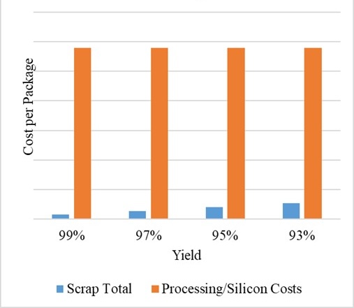
When the yield of the entire process is high, the total scrap cost is very small in comparison to the cost of the silicon (counting the bottom wafer and top dies) and the cost of processing. However, while the top die are assumed to come from a mature node and therefore not carry a high cost, the bottom wafer is expensive, assumed to come from a more advanced node. As the yield drops in 2% intervals, the scrap cost visibly rises. In the 93% package yield case, scrap cost represents almost 10% of total package cost.
Conclusion
Activity based cost modeling was used to analyze a face-to-back chip-on-wafer hybrid bonding package. The main cost drivers associated with this process, when the scope is to start with two wafers and end the analysis after the bonded stack has been diced into a package, were shown to be the creation of TSVs, hybrid bonding metallization processes, and the hybrid bonding activity itself. A key takeaway related to hybrid bonding is that the activity is not a major cost driver on a per package basis, but when evaluating a design with many small die placements per wafer, hybrid bonding does show up as a cost driver when considering the full cost per wafer.
Yield analysis showed that small yield changes have a notable impact on final package cost when the silicon at risk is not from a mature node. The smaller the die and/or package, or the cheaper the incoming silicon, the less impact to be expected from yield.
References
[1] Assured Systems, “Understanding 3D Chip Stacking,” FAQ Section of website, accessed December 2024.
[2] T. Quan, “Making SiP happen in 3D,” Tech Design Forum, December 2009.