
Is the Wild West becoming America’s center of microelectronics innovation? Based on the current wave of activity across the semiconductor supply chain, it’s starting to look that way. I’m not just talking about TSMC’s gigafab, or Intel’s expansion, although these industry giants have a lot to do with what’s happening in Arizona right now. Everyone – from academic and research institutions to equipment and materials suppliers, design tool, and technology providers – is getting involved.
Companies like Motorola, Intel, and Sandia National Lab made semiconductor manufacturing a mainstay industry in Arizona and New Mexico since the early days. But now, in part due to the new infusion of funds expected from the CHIPS and Science Act, everyone – from academic and research institutions to equipment and materials suppliers, design tools, and technology providers – is getting involved. It’s no wonder our member companies, Edwards and YES decided to open state-of-the-art facilities in Chandler, AZ this year.
Edward’s 200,000-square-foot facility will reportedly leverage the latest manufacturing and digital technologies for efficient and environmentally sustainable chip production. Edwards provides vacuum and abatement systems that are essentially “clean air machines” and vital to removing nasty chemicals and gasses used in semiconductor manufacturing. The company expects this new facility will create 300 local jobs.
And YES recently held a ribbon-cutting ceremony for the YES Advanced Technology Center (YATC), which will include, 50,000 square feet of manufacturing space, a 10,000 square foot cleanroom in the first development phase that will be expanded to approximately 40,000 square feet in the future. The cleanroom will allow YES to collaborate with its customers to develop innovative processes and validate platform prototypes. The job count at YES will be approximately 100 openings.
Let’s look at some of the recent initiatives at Arizona State University that will help fuel the industry and provide a skilled workforce to fill these positions, as well as those needed at TSMC’s facility.
The Southwest Advanced Prototyping Hub
Spearheaded by the Ira Fulton School of Engineering at Arizona State University (ASU), the Southwest Advanced Prototyping Hub (SWAP) proposal was submitted in late July to the National Security Technology Accelerator as part of the Microelectronics Commons, a $1.63B Department of Defense (DoD) program funded by the 2022 CHIPS and Science Act. The purpose of the SWAP HUB is the development of AI hardware, 5G/6G, and commercial leap-ahead technologies for defense applications.
Although the proposal has yet to be approved, SWAP Hub program director, Zachary Holman, associate professor in the School of Electrical, Computer, and Energy Engineering at ASU, says the key to the group’s success so far is “implementing our vision even before the US Government decides to fund it.” ASU itself has earmarked $250K to fund four seed projects at $50K each. Partners are expected to match the funding.
So far, the SWAP HUB comprises more than 60 leading corporate, startup, academic, and national lab partners from the semiconductor and defense sectors in Arizona, New Mexico, Colorado, and beyond. 3D InCites members Deca Technologies, Lam Research, Mercury Systems, Siemens EDA, and Cadence are among the partners. I attended the first partner SWAP Hub event in July to learn more about it, and to understand our members’ involvement. Representatives from ASU and member companies spoke about their respective areas of expertise.
In her opening comments, Dr. Sally Morton, executive vice president of ASU’s Knowledge Enterprise, noted that the Southwest is already one of the nation’s key centers of microelectronics activity.
“The success of the SWAP Hub is about more than a single DoD program. It’s about all of us coming together to make Arizona and the entire Southwest Region, America’s first full, leading-edge, microelectronics cluster.” she said.
One partner vital to the success of the SWAP Hub is Sandia National Labs, based in Albuquerque NM. According to Manager Ken Dean, Sandia is the largest US government-owned captive semiconductor fab run by the Department of Energy. Sandia’s capabilities include a semiconductor fab complex and a counterfeit detection center. It also runs a robust student intern group for microelectronics advancement or SIGMA. Its goal is to simultaneously train the next generation of leaders in microelectronics and national security. ASU students are regular participants in that program.

Partners and potential partners were asked to submit technology project applications for consideration by today (August 11). They must focus on lab-to-fab prototypes targeting defense applications that can be scaled quickly from research labs to commercial fabrication and onto a defense platform, as the Microelectronics Commons is funded by the DOD.
Department of Defense is now evaluating the hub proposals and is expected to announce the funding awards before the end of the federal fiscal year at the end of September.
ASU’s Adjacent Microelectronics Activities
We’ve seen some bumps in the road caused by a global semiconductor talent shortage. TSMC has reportedly delayed production in its Arizona fab to 2025, due to a shortage of skilled workers. Part of the issue is the disconnect between university engineering programs that don’t adequately prepare graduates for careers in semiconductor manufacturing. To address this shortage, particularly in Arizona, ASU has announced several initiatives – one with semiconductor equipment manufacturer Applied Materials and the other with TSMC.
The alliance with Applied Materials, aided by the Arizona Commerce Authority, will create a world-class shared research, development, and prototyping facility in ASU Research Park. Dubbed the Materials to Fab (MTF) Center, this $270 M investment will include a state-of-the-art 300mm fab, giving students and faculty the opportunity for hands-on learning and research on the same 300mm equipment used in leading-edge production fabs.
“This is the beginning of a reconfiguration of the way to accelerate discovery and translational research outcomes in response to real-world challenges and the development of next-generational processes, materials, equipment, and workforce,” noted Michael Crow, ASU President.
Additionally, Applied Materials plans to create an endowment fund that will provide scholarships to first-generation and/or underrepresented minority students in the Fulton Schools of Engineering, as well as opening its Momentum Fund to ASU Students. The Momentum Fund provides grants to women pursuing undergraduate degrees in engineering as they approach degree completion, helping to overcome potential financial barriers and accelerating access to careers in the semiconductor industry.
ASU has also expanded its partnership with TSMC that began in 2020, recruiting ASU graduates and training them in Taiwan, with the intention of working at the new Phoenix fab. The new partnership agreement is focused on student support, training and recruitment, and faculty work projects and research with the goal of deepening the relationship between ASU and TSMC. More details are available here.
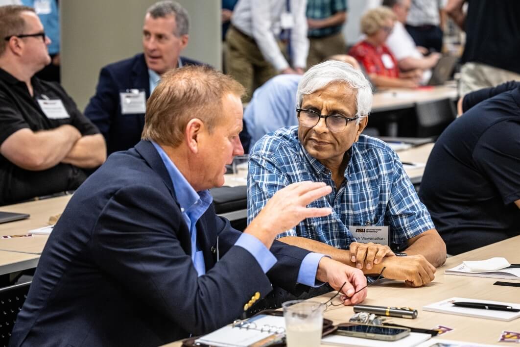
Feature photo above: Tim Olson (left), founder and CEO of DECA in Tempe, chats with Vish Viswanathan of NXP Semiconductors during a break at the Southwest Advanced Prototyping Hub workshop. (Photo by Charlie Leight/ASU News)


