
SK Hynix Advanced Packaging
Ki-ill Moon, head of Packaging Technology Development at SK Hynix recently wrote an article for EE Times entitled “ The Value of Semiconductor Packaging Technology in the Era of Heterogeneous Integration” that is certainly worth taking a closer look at.
The theme of the article is the same one that we have been preaching on IFTLE for several years, i.e. that as demand for high-performance semiconductors increases, the semiconductor market is paying more attention to the importance of the “packaging process”. In line with this trend, SK Hynix is mass-producing advanced packaging products based on HBM3 while focusing on investing in production lines and securing resources for the development of future packaging technologies.
I especially liked their take on “the history of packaging” which they divide into three major eras.
In the beginning, a package carried only one chip. Consequently, packages were simple and the value added by packaging technology was low. However, in the early 2000s, with the switch to fine-pitch BGA packaging, the incorporation of multiple chips in one package began, i.e. the “Era of Stacking Competitiveness.” As chips began to be stacked, the form of the package diversified and various derivative products were created depending on the combination of the memory chips. The multi-chip package (MCP), which implements DRAM and NAND in the same package appeared at this time.
The second era began after 2010 when a method of interconnection using a bump on a chip appeared. (IFTLE must disagree here since bumping really began to take hold post-2000, not 2010…maybe they are talking specifically about memory devices which did start to use bumping technology later.) As a result, changes in the operating speed and the device property margins occurred. They call this period the “Era of Performance Competitiveness” as packaging technology prior to 2010 generally involved connecting by wire bonding, but the introduction of bumps shortened the signal path and achieved faster speeds. Meanwhile, stacking technology using through silicon vias (TSVs) drastically increases the number of Input/Output (I/Os), which leads to connecting 1,024 wide I/Os enabling high operating speeds even in low voltage. In this era of performance competitiveness, the properties of chips change according to the packaging technology, and this becomes an important factor in fulfilling the requirements of the customers.
The third era began ~2020 and is based on all the previous packaging technologies. It can be considered the “Convergence Era” as it requires technology that can connect various types of chips into one package and, also, connect many parts into one module when incorporating a system. In this era, packaging technology itself can become a system solution, and customized packaging solutions can be provided to customers to make small-quantity batch production possible. At this point, merely owning packaging technology will determine the success of a business.
As the success or failure of a business can depend on the presence or absence of packaging technology, the value of packaging technology has continued to grow.
SK Hynix Packaging Technology
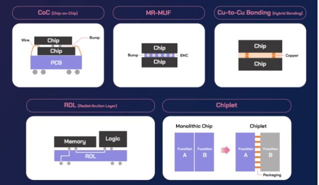
SK Hynix’s packaging technology is described as having undergone significant development throughout the aforementioned eras. Although the company‘s packaging technology was not significantly differentiated up to the stacking competitiveness era, as the performance competitiveness era began, SK Hynix became known for its packaging such as chip-on-chip (CoC) technology. Additionally, SK Hynix developed MR-MUF technology, which applies a molded underfill (MUF) material that has high thermal conductivity. It has been applied to HBM products. This advancement has helped SK Hynix increase its share of the HBM market and eventually take a leading position in the HBM3 sector.
Today, in the convergence era, SK Hynix is promoting the development of hybrid bonding technology, which uses direct Cu–to–Cu bonding. Hybrid bonding technology allows for finer pitches and, has an advantage in terms of the height of the package as it is a gapless bonding technique that does not use solder bumps when stacking chips. In addition, Fan-out RDL technology is applicable to various platforms, so SK Hynix plans to use it when incorporating packages with chiplets. SK Hynix aims to secure RDL technology below 1 micron, or at sub-micron level, by 2025.
Integra Technologies
Well, it looks like more on shoring/advanced packaging expansion is setting up shop in the American heartland.

Founded in Kansas 40 years ago, Integra, an employee-owned company with operations in Wichita Kansas, and Silicon Valley, claims to be the largest U.S. OSAT. They provide OSAT services to critical infrastructure sectors such as the military, aerospace, medical, aviation, automotive, commercial, and industrial.
Integra has just announced that Kansas had approved Integra’s economic expansion incentive application that will reportedly create > 2,000 jobs, build a 1MM sq ft headquarters and production facility and invest $1.8 B in capital in the Wichita region contingent on receiving federal CHIPS for America funding.
This Kansas incentive package reportedly paves the way for the company’s application for CHIPS and Science Act funding. Integra’s expansion plans are “…designed to address recent risks identified in the U.S. semiconductor supply chain, support the domestic semiconductor ecosystem, and strengthen advanced manufacturing in the State of Kansas”.
While Governor Laura Kelly reportedly stated “… Partnering with Integra will secure Kansas’ rightful position as a global leader in the semiconductor sector ”, IFTLE sees that as a bit arrogant. It is no one’s “right” to be a global leader in the semiconductor sector…at best it is their desire…
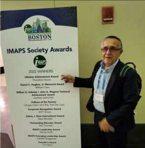
In order to deliver on such lofty goals, Integra has astutely brought on Industry stalwart Ted Tessier to serve as CTO for advanced packaging. Ted has a long background in advanced packaging including CTO at Flip Chip Int, Sr. Dir. of Wafer Level Packaging at STATSChipPAC, VP of Emerging Packaging Technologies at Amkor, and several years at Motorola Phoenix.
Recall Tessier recently won the Packaging Lifetime Achievement Award from IMAPS this past fall in Boston.
For all the latest in advanced packaging, stay linked to Insights From the Leading Edge (IFTLE)…