
Minneapolis, Minnesota — January 29th, 2021 — CyberOptics® Corporation (NASDAQ: CYBE), a leading global developer and manufacturer of high-precision 3D sensing technology solutions, will feature the WX3000™ metrology and inspection system with MRS™ sensor technology, and high-precision sensors for semiconductor tool set-up and diagnostics at the Virtual SEMI Technology Unites Global Summit from February 15-19th.
Tim Skunes, VP of R&D at CyberOptics, will share a related technical presentation ‘Fast, 100% 3D Wafer Bump Metrology and Inspection to Improve Yields and 3D System Integration’ on February 16th. Advanced Packaging (AP) and wafer level packaging (WLP) continue to be among the most dynamic and rapidly evolving areas of semiconductor development and manufacturing. As the processes and features they create have become smaller and more complex, manufacturers face an increasing need for high-precision inspection and measurement to detect defects and improve process control. This need is amplified by the fact that these processes use expensive known good die, making the cost of failure extremely high.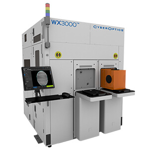
The NanoResolution MRS sensor integrated into CyberOptics’ WX3000™ system provides sub-micrometer accuracy on features as small as 25µm. While retaining its ability to reject spurious multiple reflections, it adds the ability to capture and analyze specular reflections from shiny surfaces of solder balls, bumps and pillars, allowing highly accurate inspection and 3D metrology of these critical packaging features. Complete 100% 3D/2D inspection and bump metrology can be accomplished vs. time-consuming alternative methods that require separate scans for 3D and 2D, or a sampling only approach. With data processing speeds in excess of 75 million 3D points per second, it delivers production-worthy throughput greater than 25 wafers (300mm) per hour, at speeds 2-3X faster.
“Whether it’s for the back-end or mid-end of the semiconductor fab, our proprietary sensors and systems deliver significant benefits to customers in terms of improved yields, processes and productivity,” said Dr. Subodh Kulkarni, President and CEO, CyberOptics, “Compared to other solutions, our technology saves our customers significant time and expense.”
The company will also digitally demonstrate high-precision sensors that process and equipment engineers use in the front-end of the fab to speed equipment qualification, shorten equipment maintenance cycles, lower equip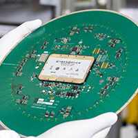 ment expenses and optimize preventative maintenance plans. The WaferSense® Auto Resistance Sensor™ (ARS) enables real-time resistance measurements of plating cell contacts in semiconductor Electrochemical Deposition (ECD) applications, and the In-Line Particle Sensor™ (IPS) detects, monitors and enables troubleshooting of particles down to 0.1 µm in gas and vacuum lines in any areas of the fab 24/7.

The Technology Unites Global Summit brings together the global microelectronics supply chain, manufacturers and end users for a digital experience featuring industry thought leaders and high-value technical content from around the world. CyberOptics is a platinum sponsor.