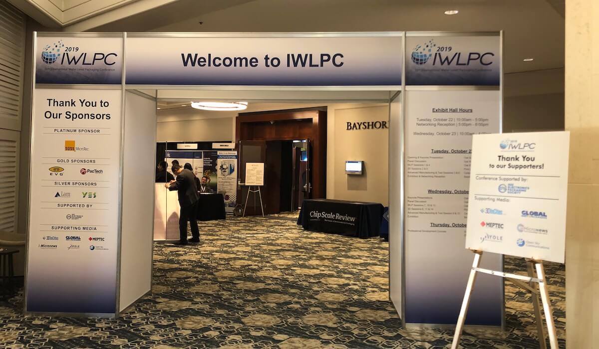
Anyone whose anyone with a hand in the evolution of wafer level packaging will be in attendance or exhibiting at the 16th Annual International Wafer-Level Packaging Conference (IWLPC) and Tabletop Exhibition next week. 3D InCites will be there and we’re excited to engage and learn from the industry’s most respected authorities addressing all aspects of wafer-level, 3D device packaging, advanced manufacturing and test technologies.
Together with Chip Scale Review and SMTA, the IWLPC has been at the forefront of packaging technology development. The conference has a rich history of bringing together attendees from over 16 countries to the heart of Silicon Valley to immerse themselves in the latest technology and business trends. This year, more than 750 attendees will be enlightened by 75+ industry suppliers showcasing their innovative products and services, including vendors from leading semiconductor companies, foundries, and OSATs, as well as key technology, equipment, and materials suppliers.
The conference is host to three parallel technical tracks with two full days of presentations on wafer-level packaging, 3D integration, and advanced manufacturing and test. Also on the agenda are numerous workshops, keynote speakers and panel discussions.
Keynote Speakers include:
Tuesday, October 22, 2019 | 9:00am
The OSAT’s Dilemma and the Future
Choon Heung Lee, Ph.D., CTO
JCET
Wednesday, October 23, 2019 | 8:15am
Slowdown: When Did it Start… What Drove it… When Will the Recovery Come
Dan Hutcheson, CEO
VLSI Research
Wednesday, October 23, 2019 | 4:00pm
A Borderless Future for Electronic Interconnect
Tim Olson, Founder & CTO
Deca Technologies
Among those giving technical presentations are…
Thom Gregorich from ZEISS.
Non-destructive 3D X-ray Characterization of a Smartwatch with Embedded Fan-out Package
Thom Gregorich of ZEISS will present how a new type of 3D X-ray microscopy inspection and measurement methodology is used to characterize the 2019 Galaxy Watch application processor module PLP-POP design. Thom will share how the data was extracted non-destructively from the intact watch PCB and application processor module and used to measure critical dimensions and assess key characteristics of the product.
Richard Barnett from SPTS Technologies.
Improved Semiconductor Device Reliability from Plasma Dicing
Richard Barnett, Senior Product Manager – Etch
Wednesday 23rd October, 14:00pm – Session 13 WLP track
IWLPC info:
October 22-24, 2019
DoubleTree by Hilton San Jose
San Jose, California, USA


