
Is GlobalFoundries looking for an exit or simply shedding parts of the company that do not fit its new focus? Back in IFTLE 406 we started discussing the persistent rumors that GlobalFoundries might be “chopped up on the auction block and its businesses sold to specialty foundries that want to supply in those specific areas.” There have been rumors that Abu Dabi Investment Corp. (ADIC), the investment arm of the Abu Dabi government has been looking to unload their stake in GF since their announcement last year that they were going to stop pursuing advanced nodes and the subsequent announcement that AMD was shifting to TSMC for future node chips.
A Steady Divestiture of Foundry Facilities
GlobalFoundries announced in February that it had agreed to sell its Fab 3E in Singapore to Vanguard International Semiconductor (VIS) as part of a broader plan to exit the MEMS business by the end of the year. The deal will be a wholesale handoff to Vanguard, and both the customers that use the fab and the personnel that work there will be transferred to the new owner. For their part, selling the fab and exiting the MEMS business will allow GlobalFoundries to raise the capital it needs upgrade its other fabs, as well as further invest in technologies that are used to make chips using the company’s other specialized manufacturing processes.
Under the agreement, GlobalFoundries will sell Tampines, Singapore Fab 3E to Vanguard for $236 MM by the end of the year. The fab is used to make microelectromechanical systems (MEMS) as well as analog/mixed-signal chips. Fab 3E has a production capacity of 35K 200mm wafer/month. Vanguard will also acquire GlobalFoundries’ MEMS-related IP. And the Global Foundries customer base.
GlobalFoundries will receive $236 MM which it will reportedly invest in its remaining RF, embedded memory and advanced analog businesses. CEO Tom Caulfield was quoted as stating: “This transaction is part of our strategy to streamline our global manufacturing footprint and increase our focus in Singapore on technologies where we have clear differentiation such as RF, embedded memory and advanced analog features……..Consolidating our 200mm operations in Singapore into one campus will also help reduce our operating costs by leveraging the scale of our gigafab facility in Woodlands …”
In March rumors persisted that GlobalFoundries 300mm Fab 7 in Singapore was for sale with Samsung and China-based chipmakers through third-party investment funds being potential buyers. Industry observers said it would easier for GlobalFoundries to sell its facilities piecemeal than the entire company in one single deal if GF were indeed seeking a full exit strategy.
In April, ON Semiconductor agreed to buy GlobalFoundries 300mm Fab 10 fab in East Fishkill, NY for $430MM. The fab is used to process 300-mm wafers using various technologies, including 45nm and 65 nm technology nodes. ON will receive the engineering staff, as well as a technology transfer, development, and license agreements. ON will start using the fab in 2020.
In April, Marvell announced that they had entered into an agreement to purchase Avera Semiconductor, the ASIC business of GlobalFoundries. IBM had sold the operation to GlobalFoundries in 2015. Marvell will pay GlobalFoundries $650 MM at closing plus an additional $90 million if certain business conditions are satisfied. The transaction is expected to close by the end of 2020 pending regulatory approvals. Marvell will inherit ~ 800 engineers focused on ASICs.
This is the third asset sale that GlobalFoundries has done in the last several months.
GlobalFoundries becomes a Boutique Foundry
With these divestitures and the announcement that GF will not be doing work on next-gen nodes, IFTLE now considers GF as having joined the ranks of second-tier foundries as a boutique foundry offering CMOS, FinFET, and the FD-SOI offerings.”
While all these moves are being “spun” as conforming to the plan of CEO Caulfield, which they certainly are, the real question appears to be whether Abu Dabi finds it acceptable to be a second-tier specialty fab. Is that really what they wanted when they began this journey and is that what they will accept now? I guess we will see in time.
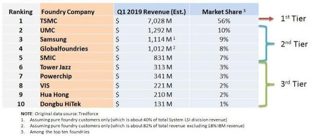
Q1 2019 Foundry rankings from Trendforce are shown in Figure 1. With their recent divestitures, GlobalFoundries is expected to fall below SMIC and out of the global top 5.

Further Cree Plans for SiC
In IFTLE 410 we looked at Cree’s plans to expand the SiC market due to automotive demand for electronic vehicles. Following up on that, Cree has recently announced a major SiC expansion in NC, based not only on automotive but also photovoltaics (PV) where SiC holds promise for inverters, by allowing for smaller chips with greater power density as well offering a greater switching frequency, meaning fewer of the “passive elements” that make inverters big, bulky and expensive.
Cree says that the new factory will create a 30x increase in its SiC production capacity by the time it is online in 2024. It may also help the move to 200mm wafer production, although initially, the factory will put out 150mm wafers. Market focus is reportedly EVs, 5G networks and inverters.
Specifically, Cree plans to invest $450 MM in its North Fab, $450 MM in the adjacent mega factory, and $100 MM in other investments related to the business…or close to $1B. Cree notes that it will be using mostly refurbished tools to build the new fab.
Optical Phased Arrays by Wafer Scale 3D Integration
UC Berkley and MIT presented an interesting joint paper at the recent IEEE ISSCC meeting.
The realization of a low-cost and robust optical beam-steering platform is a key enabler for a number of applications, including light detection and ranging (LIDAR) and free-space optical communications (FSO). Optical phased arrays (OPAs) have emerged as a promising solution, due to advancements in photonic integrated circuits (PIC) foundry processes, which have enabled high-precision fabrication of PICs with a large number of components.
In the majority of prior OPA demonstrations, only the optical components have been implemented on a PIC chip, with phase-shifting elements driven by separate discrete electronics. With the electronics integrated on a separate chip, the number and density of I/O connections required for large-element-count OPAs limit the scalability of multi-chip solutions. This issue can be addressed by monolithic integration, where both photonics and electronics are integrated on a common SOI CMOS substrate. However, monolithic integration limits the photonic device design due to CMOS design rules, available materials, and processing steps.
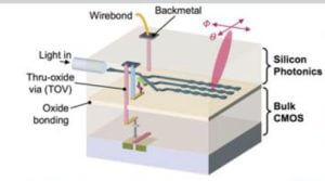
The authors have overcome these issues by implementing a wafer-scale 3D integration packaging platform, which allows for photonics and CMOS electronics to be independently optimized while enabling flexible, dense connections between them. A cross-section of the device is shown in Figure 2.
For all the latest in Advanced Packaging stay linked to IFTLE……………………………………..