
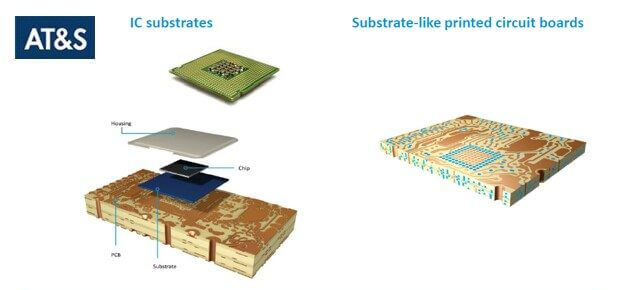
Substrate-like PCBs (SLP) is a term describing a high-density printed circuit board (PCB) that has feature sizes close to that of an IC substrate. The main difference between a PCB and an IC substrate is the feature sizes, especially line and space (L/S). SLP requires line width/line spacing equal to or less than 30/30 mm, which allows for reducing the size of the main board, thus making space for other components.
Increasing demand from end-users for thinner/compact but more functional smartphones requires a constant reduction in the board area. Such a reduction in board area would, for instance, allow implementing a larger battery. Smartphone manufacturers such as Apple and Samsung have recently adopted SLP with 25/25 and 30/30 =µm line/space (l/s) in their smartphones. Other smartphone providers such as Huawei, Oppo, and Xiaomi are also expected to adopt SLP. SLPs also are finding application in computing and communications, automotive, and medical devices. Apple has already used SLP in its Apple Watch devices.
With more smartphone manufacturers looking to adopt substrate-like PCBs in their high-end models, and other mobile devices looking to incorporate SLPs, SLP growth is expected to be significant. It is reported that there are already two China-based firms engaged in the design of new models equipped with SLP.
Zhen Ding Technology, reportedly among the suppliers of Apple, has discussed their vision of SLP demand for smartphones, wearable and other mobile devices requiring an ultra-thin and lightweight profile. The use of SLP enables them compact design without sacrificing the computing performance.
Zhen Ding, meanwhile, is reportedly planning to build additional new SLP production lines at its factory site in China.
In early 2019, Huawei reported they will follow in the footsteps of Apple and Samsung in adopting SLPs in its smartphones.
Japan’s Meiko Electronics has reportedly obtained major SLP orders from Samsung Electronics for its Galaxy devices and plans to build additional SLP production lines at its manufacturing site in Vietnam this year. Meiko is rivaling Taiwan’s Zhen Ding Technology and Austria’s AT&S in the SLP field—both of which are making SLPs for the iPhones [link].
The SLP market is expected to grow from USD 1.1 billion in 2018 to USD 2.6 billion by 2024, at a compound annual growth rate (CAGR) of 15.6% during the forecast period.
Major SLP suppliers include AT&S, TTM, Unimicron, Compeq, ZD Tech, Ibiden, and Samsung Electro-Mechanics, among others.
AT&S (Austria); TTM Technologies (US); Samsung Electro-Mechanics (South Korea); Korea Circuit (South Korea); Kinsus Interconnect Technology (Taiwan); Zhen Ding Technology (Taiwan); Unimicron (Taiwan); Compeq (Taiwan); Ibiden (Japan); Daeduck (South Korea); ISU Petasys (South Korea); Tripod Technology Corporation (Taiwan); and LG Innotek (South Korea) are among the major players in the SLP market.

Kinsus (Taiwan) is ranked first in the substrate-like PCB market (2017). In the SLP market, Kinsus is an IC substrate provider and a major supplier of substrate-like PCBs for the iPhone i8. Kinsus is also a supplier for Qualcomm, Broadcom, and Nvidia. Ibiden (Japan) is in second place in the SLP market.
COMPEQ, a supplier of Apple, spent ~ $130MM in 2017, mainly for the production of SLPs, which was used for Apple Iphone8 [link]
Samsung Galaxy S9
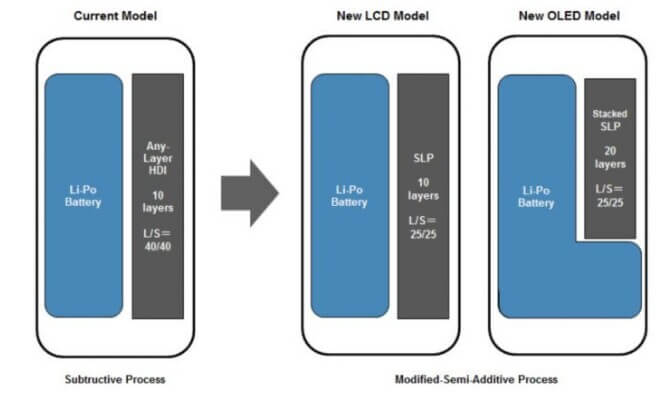
Samsung’s goal for the 2019 Galaxy S9 was to fit a bigger battery inside it [link]. A bigger battery usually means a thicker or larger phone unless you are able to shrink the size of the other components. Samsung’s approach was to switch to Substrate-like PCB which let it reduce the size of the main board, allowing a bigger battery as shown below.
Apple was the first to use SLPs in late 2017 with its introduction into the iPhone 8.
The China and Taiwan Packaging and Test Industry
DigiTimes has recently noted that the top 10 players in the global IC packaging and testing market comprised a combined 84% share of the $28billion market and that three of the top 10 players are China-based. Jiangsu Changjiang Electronics Technology, with a global market share of 13%, began its acquisition strategy early. Jiangsu Changjiang currently generates revenues of $3.64 billion a year. Tongfu Microelectronics and Tianshui Huatian Technology are also in the global top-10. The three of them hold 20% of the worldwide packaging and testing orders.
Taiwan players are still the most competitive in the packaging and testing field with ASE, SPIL, Powertech Technology (PTI), King Yuan Electronics (KYEC) and Chipbond: all top-10 players. The five firms together have 44% of worldwide packaging and testing demand, and together with other Taiwan based non-top10 participants including Orient Semiconductor Electronics (OSE) and Sigurd Microelectronics, they control over half of the global packaging and testing market.
For all the latest in Advanced Packaging stay linked to IFTLE…………………………………..

