

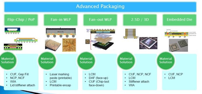
Continuing our look at presentations from the recent 2018 IWLPC conference, let’s look at the Jiw Pai Henkel presentation on advanced packaging underfills.
Henkel – Underfill Options for Advanced Packaging
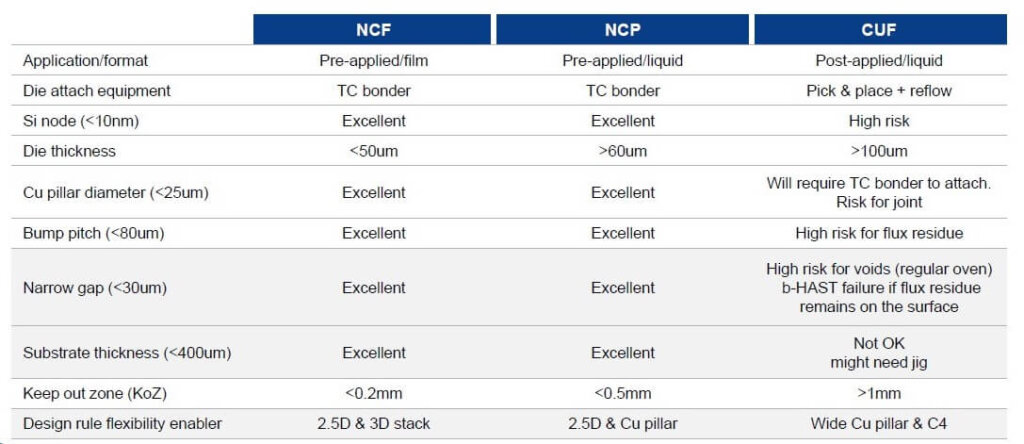
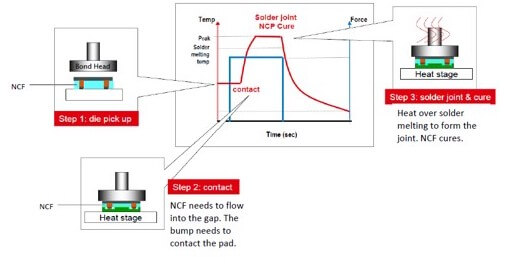
Bai and co-workers examined the use of capillary underfill (CUF), non-conductive paste (NCP) and non-conductive film (NCF) in advanced packaging applications (Figures 1 and 2).
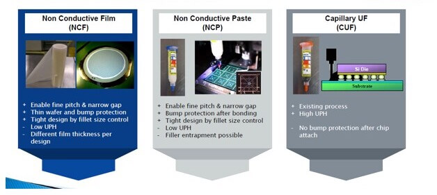
Each of these technologies has its sweet spot in terms of throughput, cost, yield, and performance as shown below:
IFTLE has always been a strong supporter of NCF. Key requirement for NCF include;
- Soft film to laminate bumped wafer
- Transparency for bump recognition
- Fast cure to hold the die in place after TC bonding
- High Tg & Low CTE for thermal cycle reliability
- Filler particle size control for film transparency
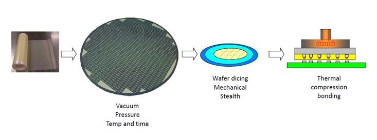
The typical NCF process flow is shown in Figure 4.
JEDEC has announced an update to JESD235 the high bandwidth memory (HBM) DRAM standard. JESD235B for HBM leverages wide I/O and TSV technologies to support densities up to 24 GB per device at speeds up to 307 GB/s. This bandwidth is delivered across a 1024-bit wide device interface that is divided into 8 independent channels on each DRAM stack. The standard can support 2-high, 4-high, 8-high, and 12-high TSV stacks of DRAM at full bandwidth to allow systems flexibility on capacity requirements from 1 GB – 24 GB per stack.
This update extends the per-pin bandwidth to 2.4 Gbps, adds a new footprint option to accommodate the 16 Gb-layer and 12-high configurations for higher density components
HBM DRAM is used in graphics, High-performance computing, server, networking and client applications where bandwidth, bandwidth per watt, and capacity per unit area are important parameters. JESD235B is available for download from the JEDEC website.

Intel foundry business – Digitimes
Monica Chen, of DIGITIMES reports that Intel’s recent announcement about refocusing its manufacturing resources on its own products is fueling speculation in Taiwan that Intel may discontinue its custom foundry business. Unnamed Taiwan industry contacts stated that Intel, while in the contract chipmaking market for years, has not been focused on competing with TSMC or Samsung. One Taiwan source stating “…their foundry business exists in name only, with no major clients or large orders recorded.”
Speculations about Intel quitting the contract manufacturing sector have appeared periodically with no response from Intel. It entered the market in 2010 mainly to optimize the adjustment of its own manufacturing capacities. In addition, tight 14nm and 22nm capacities have been preventing Intel from taking contract foundry orders. At their Technology and Manufacturing Day in 2017, Intel reportedly promised that it would help customers access their technology and manufacturing resources. But… the release of Intel’s 10nm platform has been long delayed, with current speculation that it will not come till the second half of 2019. This has disrupted the advance of Intel’s own products to 10nm and tightened the supply of 14nm and 22nm CPUs to customers.
TSMC is now clearly leading the development of advanced process technologies. They have entered volume production of a 7nm process in late 2018 and will have completed over 50 tape-outs for the process by the end of the year. They are now reading production of a 7nm process. They currently project 5nm volume production in 2020, and its planned 3nm fab is set for an official run in 2022.
Samsung recently announced completing the development of 7nm LPP (low power plus) process, which will soon enter commercial run. But industry sources said Samsung has yet to land orders from any major customer for chip fabrication using the latest process. So far, Apple has placed all 2019 orders for its A13 mobile processors with TSMC.
For all the latest on Advanced Packaging stay linked to IFTLE……………………


