

 Today’s SoCs, multi-core CPUs and GPUs with their high performance, high bandwidth interconnect interfaces put demanding challenges across the entire system signal path, requiring system-wide optimization for product success. However, although typical system substrate design discipline (chip, packaging, and PCB) have well-developed design approaches, the interaction between them largely remains isolated and undeveloped.
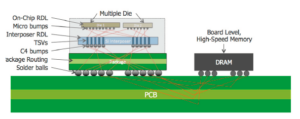
Often the bridge between the chip and system PCB, the IC Packaging offers the best opportunity for optimizing signal performance, power delivery/integrity and interconnect optimization. Using a multi-substrate design approach, simulation becomes an easily reachable reality, from the chip’s buffer block through package routing and on through system PCB implementation. By optimizing critical and key signal down interface paths throughout the system will result in far fewer downstream issues that will require resolution.
The traditional path to system design is to know what you need to build, to identify what must be done, and then to design to those requirements. The defense and aerospace industries have had great success enforcing this method of constrained design, especially for complex system designs where the correct-by-construction approach speeds design time, improves quality and lowers costs by reducing design iterations.
As next-generation High-Density-Advanced-Packaging (HDAP) designs become more common, PCB designers and engineers can use system-level co-design to tie multi-substrate visualization, planning, and optimization, into a complete multi-board design.

Completing a package layout with these techniques and steps ensures the best end design possible. But, before you build and test it in the lab, try simulation for a quick and less expensive approach to finding unexpected signal integrity issues and ensuring that your design will operate as planned.


