
 On March 15, 2017, TSMC held its 23rd Symposium, based on popular request, at the Santa Clara Convention Center. I had the opportunity to attend the entire symposium and want to share some of my impressions and facts learned with you.
TSMC, by far the biggest pure-play foundry, has pioneered the transition from integrated device manufacturers (IDMs) to the fabless and foundry business model and has since continued to recognize emerging opportunities early and execute quickly to meet the new market requirements. Last week’s symposium, TSMC re-emphasized the message that the “smartphones era” is no longer the main driver for semiconductor innovation. Rather, automotive, high-performance-per-Watt computing (HPC), wearables and a broad range of internet of things (IoT) applications, as well as their supporting infrastructure requirements, will drive technology advancements, revenue, and profit growth. All the TSMC presenters conveyed that they are well positioned to benefit from the significantly changing semiconductor market requirements and, to my personal delight, even have a strong back-end capability to serve the market needs for multi-die IC assembly and test.
In his opening remarks, Rick Cassidy, Sr. VP TSMC, and President TSMC North America thanked the many attending customers for their business and the 47 exhibiting partners for their cooperation. He proudly announced that in 2016, North America was again the largest market for TSMC, contributing 71% of total revenues. Cassidy highlighted that TSMC’s wafer fabs manufactured 5.8 Million 12” equivalent wafers for 5238 application-specific products, and hinted that to a large extent, it’s his responsibility to fill TSMC’s continuously expanding fab capacity.
Mark Liu, president, and CoCEO re-emphasized TSMC’s mission to be “the trusted technology and capacity provider” without any competitive element to TSMC’s currently 450 active customers. Liu briefly talked about the wide range of technologies TSMC offers to serve primarily four major market segments: Mobile, HPC, automotive, and IoT. Like all other TSMC speakers, he demonstrated that TSMC’s planning and development focus is not only technology-centric but becoming more and more applications-focused. An integral part of Liu’s 50-minute speech were also testimonials from key executives at Cirrus Logic, Dialog Semiconductor, Silicon Image, Nvidia, Analog Devices, Renesas and STMicroelectronics, all appreciating TSMC’s capabilities and cooperation.
After a brief networking break, Y.J. Mii, Sr. VP[if !supportAnnotations][G54][endif] R&D and Technology Development, opened his speech by re-introducing TSMC’s focus on serving the four segments mentioned above. He confidently announced that 7nm risk production will start in Q4, 2017; selective EUV deployment in Q2, 2018; 5nm risk production in Q2, ’19; and 5nm high volume production in 2020. Mii also showed a cross section of nanowire transistors out of their R&D line and mentioned TSMC’s work on Tunneling FETs. In addition to pushing feature sizes, TSMC is working on a range of specialty technologies, like eMRAM and eRRAM as well as improvements to image sensor and MEMS technologies. In support of the automotive market, TSMC will introduce a 7nm technology for up to 150°C operating temperature and offer Spice models characterized up to 175°C. Mii also emphasized TSMC’s commitment to wafer-level integration and several new integrated fan-out (InFO) packages, to capture the growing system-level integration opportunities.
Cliff Hou, VP R&D, Design, and Technology Platforms, outlined the progress TSMC is making, together with design enablement partners, to complement TSMC’s technology thrust following Moore’s Law with EDA tools and IP building blocks. Equally important, Hou showed the design enablement work in support of More than Moore market requirements for InFO PoP, chip-on-wafer-on-substrate (CoWoS) and 3D ICs.
In addition to presenting many tables listing which EDA tools are qualified for which process technologies, Hou proudly talked about the key steps of TSMC’s chip-package co-design flow. Going even a step further, he explained how GUC, Hynix, and TSMC have worked together on a JEDEC compliant SiP reference design, comprising an ASIC and HBM2 memory cubes on an interposer. TSMC’s deep sub-micron designs are not only significantly increasing in numbers but also in complexity. To make an IC designers’ work a bit easier, TSMC has already deployed Machine Learning (ML) technology in the design flow for clock-gating and post-route improvements and demonstrated ML’s value on a recent 7nm design with ARM cores 72 and 73. A very innovative step.
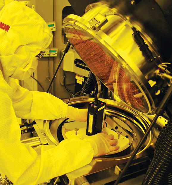
JK Wang, VP Operations, 300mm Fabs, also mentioned that his department benefits from Big Data and ML to manage the 20 to 60 process technologies per fab, serving 50 to 100 customers with 500 to 1500 products. He announced that TSMC’s Wafer Fab in Nanjing will start production in Q4, 2018. While total TSMC’s wafer fab capacity will increase by about 10% this year Wang projects that 10 and 7nm capacity will grow 2x in 2017, followed by a 3x capacity increase in 2018. Wang also talked about TSMC’s three backend fabs under his management and emphasized their importance for heterogeneous system integration.
Rick Cassidy summarized the morning sessions by highlighting these five points:
- TSMC continues to push Moore’s Law and sees 7nm technology as very well received by customers
- TSMC also invests significantly in specialty technologies to give electronic products the ability of humans’ five senses
- The advanced back-end fabs support customers with packaging capabilities for (heterogeneous) system integration
- Design enablement gives customers the ability to optimize their products quickly and efficiently
- TSMC’s manufacturing excellence demonstrates vision and provides capacity
After the lunch break, BJ Woo, VP Business Development, shared some of her market observations and key projections, e.g.:
- Phones will show 7%, high-performance computing 10%, Automotive 12% and IoT 25% CAGR in the next several years.
- By 2020 artificial intelligence, natural interfaces and high security will be important features for electronic products
- By 2020 high bandwidth, parallel processing, 5G, and infrastructure technologies will gain in importance
- ICs, serving primarily passive safety and entertainment today, will make cars smarter, greener and much safer by 2020.
- To win in the growing market for wearables, ultra-low power, sensors, connectivity, and security are needed.
Ms. Woo also outlined how TSMC’s broad range of technologies apply to specific market segments and application requirements, quantified the efforts needed to migrate designs from one of TSMC’s many technologies to another and the speed/power/cost benefits of such transitions. Clearly, very useful information for IC designers, marketing, and management at TSMC’s customers.
Before the next speaker, Suk Lee, Senior Director, Design Infrastructure Marketing, took the stage, a significant number of people left the room, … hopefully to talk with some of the 47 exhibitors. This “migration” showed me that many IC designers still see design enablement as a job for the corporate CAD departments, which are dwindling in headcounts and drowning in the many diverging application specific design flow needs. After seeing this “migration” I would like to ask here all designers to invest some time into learning about latest EDA and IP innovations and to prepare themselves for sharing their ideas and requirements with the EDA and IP partners, who are ready and eager to make the IC designers’ – and system designers’ – lives easier.
Lee, like all previous speakers, emphasized TSMC’s commitment to support application-specific requirements. He not only showed which design tools and IP building blocks are qualified for which one(s) of TSMC’s process technologies, but also talked about TSMC’s reference flows for mobile, automotive and other segments. Especially automotive topics got a lot of Lee’s attention. He outlined TSMC’s design enablement work to continuously improve IC Quality and reliability, guarantee functional safety and security, meet ISO 26262, AEC-Q100 grade 1 and 2, as well as their own TSMC 9000 A standard.

Last, but (from my own perspective) certainly not least, Lee presented some of TSMC’s successes and ongoing work to bring design formats and methodologies in the silicon world closer together with their previously very remote cousins from the packaging world. In cooperation with Cadence, Mentor Graphics and ANSYS, TSMC has developed a die-package reference design flow. Having been significantly involved in the development of TSMC’s IC reference design flows #1 and 2 at the end of the previous millennium and having seen these flows’ contributions to TSMC’s success in the past two decades, I consider this die-package co-design flow as a very important differentiator for TSMC. Thermal, timing, power and signal integrity challenges are just a few of the design steps that can only be solved successfully and in a timely manner with such a die-package co-design flow.
After a brief coffee and networking break, George Liu, Senior Director Sensors, and Display Business Development opened his presentation by asking: What will be the next “killer app” for Semiconductors? Will it be virtual reality (VR), augmented reality (AR), drones, robots, artificial intelligence (AI), or…?
Liu pointed out that, that whatever the “killer app” will be, it – most likely – will need Big Data, HPC, and deep learning capabilities – all opportunities for lots of semiconductor content.
However, none of these “killer apps” can really succeed without interfacing with the real world, e.g. with other drones, robots, and humans around them. Clearly, they need equivalents of the five human senses – sight, hearing, smell, taste, and touch – to perform their missions. With this intro, Liu elegantly made the case for the importance of his products: sensors and displays.
He highlighted that MEMS are growing at 30% per year and are being used to track motion, measure pressure and sense other dimensions. As recent examples, Liu mentioned sensors to authenticate a person’s fingerprint, voice, iris and other unique characteristics. Regarding displays, Liu also reminded us of the importance of touchscreen displays, the high quality and fast responding OLED displays, of borderless displays with ever increasing resolution (e.g. 1920 x 1080 growing to 3840 x 2160 pixels).
Last, but certainly not least, Douglas Yu, VP Research & Development, Integrated Interconnect & Packaging, clearly showed that TSMC is no longer only a wafer fab, but also offers wafer-level system integration in its three backend fabs.
Building on the high-profile announcement that Apple uses TSMC’s InFO_PoP IC packaging technology to stack the iPhone’s 7 Application processor and a DRAM, Yu presented several new multi-die package types available and in development. He showed the progress TSMC is making in regards to wafer bumping (even for the 7 nm process), smaller bump pitches (130 declining to 60 um), die sizes (7×7 to 10×10 mm), integration of passives into multi-die packages, reduction of line/space (2/2 to 1/1 um), larger interposers (1x to 1.5x to 1.75x reticle size), and support of larger package sizes (up to 45 x 45 mm).
Yu also mentioned TSMC’s reference design platform, combining a GCU ASIC and 4 Hynix HBM memory cubes (next step: 6 HBMs) on an interposer and TSMC’s die and package co-design flow.
Yu summarized the day’s ~ 6 hours of presentations very well with this statement: “TSMC wants to be your System Integration Foundry!”
Looking forward to your comments….Herb


Very useful article supporting Smoltek’s opportunity of shrinking multi die packaging footprint progress by a factor of 10-100x.