

In the past few months I have been reading a lot of depressing news about our semiconductor industry’s declining growth rates, shrinking profit margins, many consolidations, as well as many articles about why, when and how following Moore’s Law will be only justified for extremely high-volume designs. Sounds kind of depressing and worrisome for semiconductors, however, last week’s International Electron Devices Meeting (IEDM 2016) improved my outlook and optimism for our industry significantly.
IEDM was again professionally organized and very well-attended. The device experts’ current technological prowess and the many signs about the promising future this field offers, really impressed me:
- The average age of the 1600+ attendees was relatively young – compared to many other conferences I attended this year.
- Besides the U.S., Asia, Japan and Europe were well represented.
- The focus of session topics and individual presentations went far beyond device physics. Many presenters also talked about IC design considerations, the applications they are targeting and even the benefits they can offer end customers in specific market segments, e.g. automotive, industrial…
- Progress and promise of new memory technologies also look encouraging.
- Most IoT edge nodes will include significantly more digital functionality than expected a few years ago to limit the communications bandwidth needed. MEMS and sensors to capture physical, chemical and biological data will increase the semiconductor content as well. IoT edge nodes, equipment “in the fog” and in the cloud offer a wide range of development challenges for device experts and revenue growth opportunities for our entire industry.
- Power electronics is another relatively new field that’s challenging device and materials experts and a significant opportunity for semiconductor growth.
- The “good old” silicon is getting great company from several compound semiconductor materials, like GaN, SiC, SiGe, III-V channels on bulk…
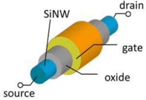
Beyond FinFET devices, gate-all-around horizontal and vertical nano-wires promise to further improve channel control and efficiency ( Figure 1) .
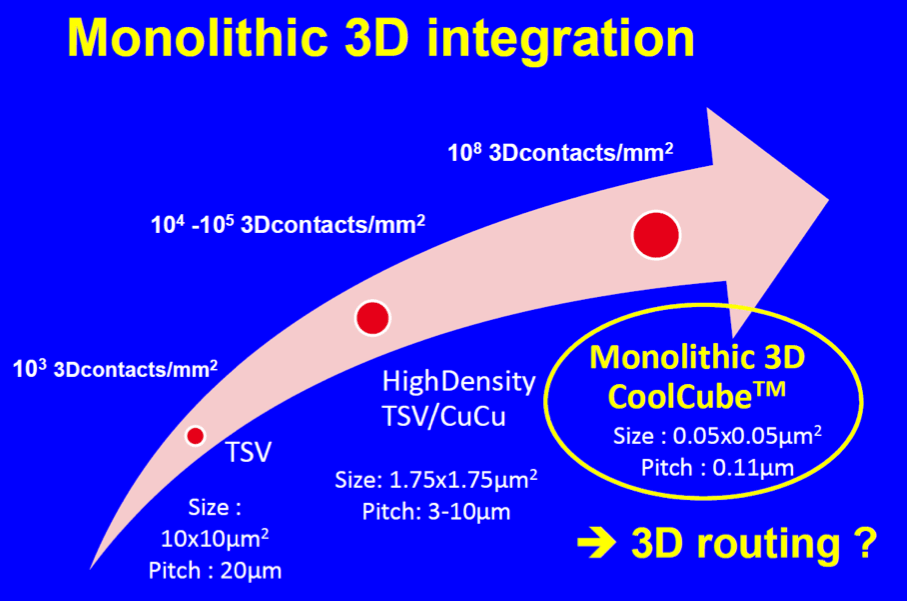
In addition to the density monolithic 3D NAND technology enables for memories, Leti’s monolithic CoolCube demonstrates impressive interconnect density for logic (Figure 2).
Many presenters conveyed at IEDM how they characterize and describe their semiconductor materials’ capabilities with equations/graphs/tables in, e.g. a PDK (Process Design Kit). They have even demonstrated the accuracy of such models and data by feeding them into EDA tools, then comparing the simulation results with actual bench test data. I hope that soon Multi-die IC assembly and test experts and their material suppliers will use similar methodologies and develop ADKs (Assembly Design Kits) to streamline communication and cooperation with IC and system designers, differentiate their IC assembly and test capabilities and, at the same time, justify higher profit margins.
IEDM even covered EDA topics, of course mostly in the T-CAD space.
After above general observations at IEDM 2016, here are highlights from two tutorials on Saturday, and the Design/Technology Enablers for Computing Applications short course I attended on Sunday, December 4:
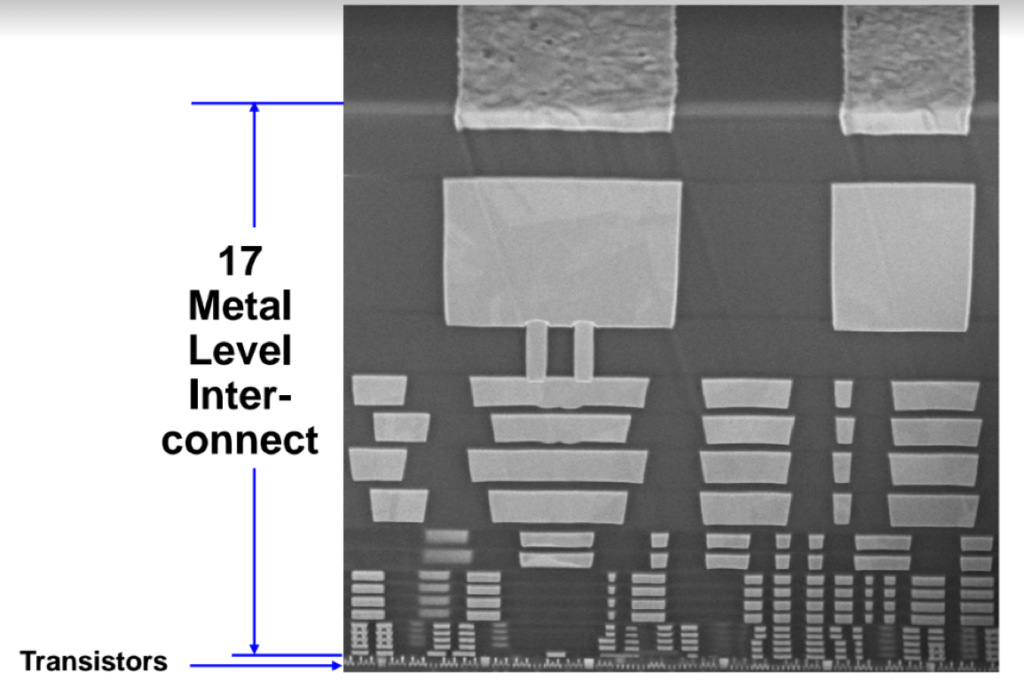
In Saturday’s first tutorial, titled The Struggle to Keep Scaling BEOL and What We Can Do Next, Rod Auger, GlobalFoundries, talked about backend of line (BEOL) challenges and showed us how big and complex an e.g. 17-layer metal stack in today’s SoCs is, compared to the tiny transistors at the bottom (Figure 3).
Auger also explained how to address a long list of system-on-chip (SoC) design and manufacturing challenges, such as power and signal integrity, clock skew, minimizing delay and power dissipation in global and detailed routing wires, reducing coupling between wires, managing electro-migration, ways to reducing dielectric constants, improving current and future alignment accuracies, etc. Clearly, Auger made me admire the engineers who can solve these increasingly difficult SoC challenges at every new process node.
Bottom line: SoC development cost and time will continue to increase. This trend will demand higher and higher production volume to achieve payback of the initial investment. I expect that utilizing the modularity of multi-die ICs (2.5/3D, WLP) will soon become a much faster and more economical way to serve a broad range of applications.
Cypress’ Ali Keshavarzi talk in the Embedded Systems and Innovative Technologies for IoT Applications tutorial about the broad range of IoT requirements. Low power dissipation/energy harvesting, small form factor, flexible architectures as well as high security, were some of the IoT challenges Keshavarzi outlined and explained how to meet them. A fascinating part of Keshavarzi’s message was a short film outlining how T.J. Rogers, Cypress former CEO, deploys humidity sensors in IoT devices to optimize very localized watering for his three vineyards.
Nvidia’s John Chen organized an all-day short course for Sunday. He won six very experienced presenters to share their knowledge about Design/Technology Enablers for Computing Applications.

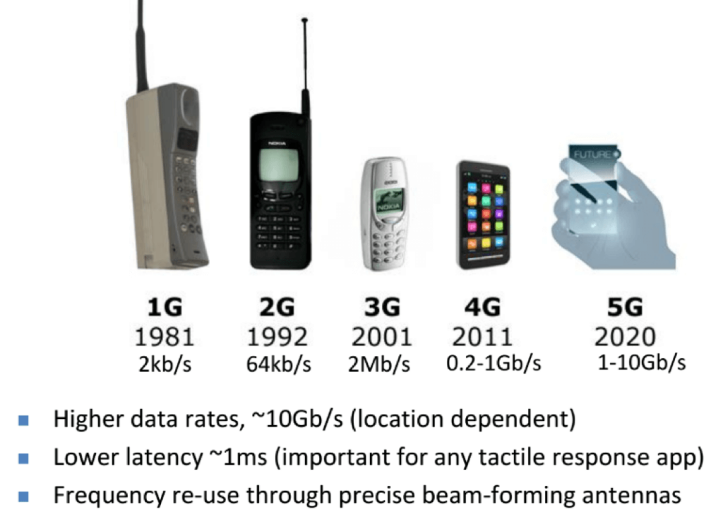
Xilinx’ Liam Madden emphasized how ubiquitous mobile devices are today and how much data they already consume and generate. He projected that the broad deployment of IoT for machine-to-machine communication will quickly add a few magnitudes to today’s digital universe of one YottaByte (= 1024 Bytes). Madden stated that data communication and compute requirements will force our industry to provide much higher performance per Watt and significantly faster communication (Figure 4). Madden also explained the need for parallel processing and the use of dedicated hardware for fast and low-power execution of complex algorithms, using e.g. FPGAs.
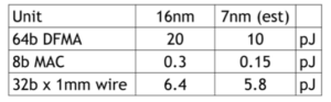
Nvidia’s Bill Dally also talked about interconnect challenges. He emphasized that the energy needed for a specific computing operation is much smaller today than the energy required to transmit the resulting data. Even worse, while computing energy scales with feature size, the energy needed to transmit data within a 2D SoC barely decreases (Figure 5).
Michael Harrad and Gabriel Molas, both from Leti in France, explained computing architectures and how to break the bottleneck between computing and today’s memory devices. They also described and compared emerging memory technologies and devices, e.g. high density and high bandwidth memory cubes.
Alberto Doronzo from Texas Instruments focused his presentation on Power management ICs (PMICs) for our high voltage power grid and showed how GaN technology will change this field with much more efficient power conversions.
Last, but definitely not least, Douglas Yu demonstrated TSMC’s current range of advanced IC packaging capabilities and the company’s commitment to serving high-performance computing and high volume mobile applications with packaging technologies that meet the specific performance, power, profile, cycle time and cost requirements (P3C2). Yu also compared TSMC’s packaging capabilities with advanced packaging technologies other major suppliers offer.
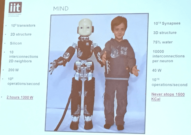
Just a few more words about another highlight of IEDM 2016: Roberto Cingolani’s keynote at the awards presentation luncheon on Tuesday.
Cingolani’s presentation, Translating Evolution Into Technology, outlined his research at the Instituto di Tecnologia in Genova, Italy. Comparing his young son’s sensory and computing capabilities, as well as energy efficiency, with the recently developed “human-like” robot fascinated the audience and demonstrated how big the gap between the capabilities of humans and robots still is (Figure 6).
LOTS of opportunities for our semiconductor industry and systems houses!!! ~ Herb


