Driven by rising demand for thinner wafers and stronger die, dicing technologies are evolving. “Reaching more than US$100 million in 2015, the dicing equipment market will double by 2020-2021”, announces Yole Développement (Yole) (Source: Thin Wafer Processing & Dicing Equipment Market report, Yole Développement, May 2016). Yet at the same time, thin wafers are creating new challenges of significant interest in the dicing equipment industry such as die breakage, chipping, low die strength, handling issues and dicing damage.
Yole’s Technology & Market Analyst, Amandine Pizzagalli, is pleased to give her vision of the dicing technologies, market forecast and competitive landscape during the webcast “Plasma Dicing for Next Generation Ultra Small and Ultra Thin Die” organized by SPTS Technologies, an Orbotech company. This webcast will take place on September 14. To register click PLASMA DICING.
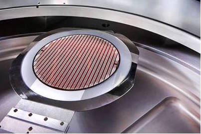
Today, the most common dicing technology applied across memory, logic, MEMS, RFID and power devices is mechanical dicing, also known as blade dicing. “Blade dicing represents more than 80% of the dicing brand equipment business in terms of dicing tools and stealth dicing 20%”, explains Amandine Pizzagalli from Yole.
However, companies are showing a growing need for thinner wafers and smaller devices in general, and Yole sees a trend towards adopting alternative dicing technologies. These include stealth and plasma dicing based on deep reactive ion etching technology. Yole’s analysts details the plasma dicing market per application:
- Memory specifically has predominantly relied on a combination of blade and laser dicing applied together to singulate complex stacks. Using only blade dicing on top layers leads to delamination issues because of the high metal density. However, it’s difficult to safely singulate 50 µm thin wafers even with laser dicing and this could allow plasma dicing to enter this area.
- “Even if the philosophy of the designers is changing, memories manufacturers are still the most conservative”, details Amandine from Yole.
- In MEMS devices, blade dicing is largely applied for singulating the ASIC, capping, and MEMS sensors. However, exposure to water from the process can contaminate some sensors and destroy sensitive MEMS structures, for example in MEMS microphones. In such cases, stealth dicing has been already adopted in large volume production.

Plasma dicing has also been adopted in low volume production today for MEMS devices.
- In parallel, the RFID is a growing market segment: plasma dicing is already in production but the adoption rate is still small. According to Yole’s analysts, a fast growth for plasma dicing, especially for RFID devices, is expected. Indeed plasma dicing has the ability to reduce die fragility, boost die strength, increase the number of chips per wafer and thus reduce Cost Of Ownership of equipment overall.
- “As die sizes continue to shrink, singulation by plasma etching offers considerable benefits for die quality and strength as compared to traditional dicing solutions,” stated Richard Barnett, Etch Product Manager at SPTS Technologies, an Orbotech company. And he adds: “Ultra-small and ultra-thin devices like RFID chips or fragile devices like MEMS are more susceptible to damage from the vibration and chipping caused by mechanical saws, or from the heat caused by lasers.”
Under its new thin wafer & dicing equipment market report, the “More than Moore” market research and strategy consulting company is analyzing the competitive landscape: the current market is today controlled by DISCO and Accretech, which today claim market shares of almost 80% focused on blade dicing and stealth dicing, respectively:
- DISCO leads the blade dicing market and offers a large product portfolio including stealth dicing and laser ablation. They have also a partnership with Plasma-Therm which gives them access to the complete range of dicing technologies: Yole’s analysts had the opportunity to discuss the market, its evolution and challenges with Abdul Lateef, CEO, and Thierry Lazerand, Business Development Director, of Plasma-Therm. To discover this interview, click Plasma-Therm solution.
- Accretech leads the stealth dicing market offering.
- ASM Pacific is a strong player in laser ablation, especially because their process does not lead to contamination issues compared to standard laser ablation technology.
During SPTS Technologies webcast, Amandine Pizzagalli will describe the today’s competitive landscape of the key dicing technologies across MEMS devices, power devices, CMOS image sensors, and RFID devices, highlighting her major findings on the evolution and trends of the dicing technologies.

These results are part of Yole’s report entitled Thin Wafer Processing & Dicing Equipment Market. Under this analysis, Yole presents a comprehensive overview of the key dicing technologies benchmarks in terms of feature requirements. This report includes insights into the number of tools, broken down by wafer size, by application and by dicing technology… A full description of the report is available on i-micronews.com, manufacturing reports section.
In parallel, SPTS Technologies speaker, Richard Barnett also proposes an overview of the latest advances in plasma dicing. During his talk, Richard will highlight the latest data illustrating how processing routes affect die strength, share experiences with different types of tapes and other die features such as solder balls. SPTS Technologies will share details of the latest equipment which is now available for plasma dicing wafers up to 300mm (on 400mm tape frames) for full production applications.
SPTS Technologies webcast will be of interest to professionals involved in the design, fabrication and/or packaging of semiconductor and MEMS devices, production engineers responsible for optimizing yield and quality of semiconductor and MEMS devices. It is also useful for design engineers and anyone wanting to learn more about the benefits of plasma dicing to improve yield and quality of semiconductor and MEMS devices.
Save the date today and register on PLASMA DICING!
Source. http://www.yole.fr