For many years now, the semiconductor industry development has been governed by Moore’s law and the increasing demand for higher performance and lower manufacturing costs. Under this context, the “More than Moore” company, Yole Développement (Yole) has identified a strong interest for panel-level packaging technologies. “At Yole, we saw a growing enthusiasm for panel package solutions dedicated to a selection of advanced packaging platforms,” asserts Amandine Pizzagalli, Technology & Market Analyst, Advanced Packaging & Semiconductor Manufacturing at Yole. And she adds: “The panel packaging market is a competitive market which is attracting lot of new entrants compared to the existing advanced packaging market segments”.
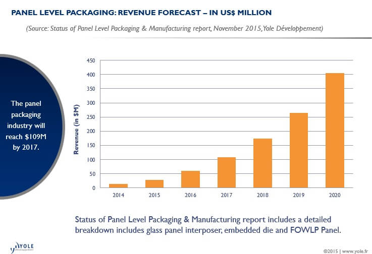
Under the new advanced packaging analysis entitled “Status of Panel-Level Packaging & Manufacturing” released by Yole last November, the market research and strategy consulting company estimates, the panel packaging industry will reach US$ 109 million by 2017, with a market value of US$ 405 million by 2020.
The aim of Yole’s report is to provide a comprehensive overview of panel-level packaging technologies available right now and in development. The analysts detailed in this report, panel-level packaging solutions for the following advanced packaging platforms: FOWLP[1] panel, embedded die, hybrid interposer and interposer (silicon, glass and organic)… For each segment, Yole’s team describes the commercial status, the market adoption and the key related applications. Analysts also identified the players for each technology and their market positioning all along the supply chain. They propose a comprehensive description of the competitive landscape as well as related market metrics.
For more than four decades, the semiconductor industry has rigorously followed Moore’s Law in scaling down CMOS[2] technologies. However, a huge investment in new lithography solutions is required to achieve advanced nodes in a range of 20nm. Although some packaging platforms processed on wafer, i.e. silicon interposer, exhibit good performance, high cost is still the main obstacle that limits its adoption for high-volume manufacturing.
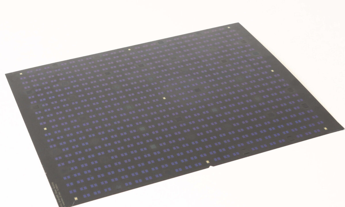
“The demand for lower cost with higher performance has driven the semiconductor industry to develop innovative solutions,” says Santosh Kumar, Technology & Market Analyst, Advanced Packaging & Semiconductor Manufacturing at Yole. And he explains: “One new approach to reducing overall cost is to switch from wafer to a larger-size panel format. Indeed, the panel infrastructure has attracted considerable interest from the semiconductor industry and is certainly a promising market due to its cost advantages and economy of scale benefits.” Panel-level manufacturing has the potential to leverage the knowledge and infrastructure of WLP[3] and the PCB[4]/Flat-Panel Display/Photovoltaic industries.
To perform this new analysis, Yole’s experts gathered valuable information at multiple levels of the supply chain: they interviewed advanced packaging leaders including device manufacturers in both volume production and development stages; they also debated with equipment and materials suppliers to get a wide vision of the panel packages technologies and understand the technical and market issues.
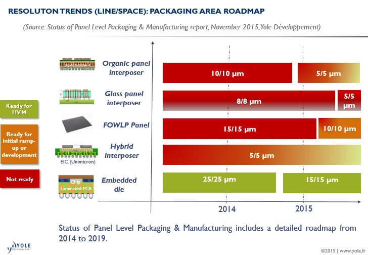
Under this approach, the market research company highlights the key insights of this industry and details the range of applications: “Panel’s application scope could be segmented into three categories defined by the required resolution,” announces Amandine Pizzagalli from Yole:
- High-end products like networks,CPU[5]/GPU[6], FPGA[7], and servers will necessitate a resolution reduced to 2µm. Therefore, this area is likely to be dominated by 300mm lines where the front-end is already well-established and has the L/S[8] capability to achieve such resolution.
- Mid-range products including base-bands, processors, power management modules, and RFIC should be the main target of FOWLP based on panel and glass panel interposers.
- And organic interposers should be restricted to low-end products: mobile, consumer, WiFi, and power management.
Business is there for the taking! But, how to design the ideal supply chain to support high-volume manufacturing…? Yole’s report provides an in-depth analysis of the panel industry, its future development and related drivers covering platforms such as FO WLP panel, embedded die, organic interposer, glass panel interposer and hybrid interposer. A detailed description of the report is available on i-micronews.com, Advanced Packaging reports section.
Yole and its advanced packaging team, are closely studying and monitoring the industry’s activities in the advanced packaging field. Yole’s vision will be presented during the European 3D Summit 2016 taking place in Grenoble, France, from January 18 to 20, 2016. The company is partnering with SEMI organization to support the European 3D Summit. The European 3D TSV Summit is organized by SEMI Europe. To meet Yole’s experts, discover the detailed program and register, click European 3D Summit.
[1] FOWLP : Fan-Out Wafer Level Packaging

[2] CMOS : Complementary Metal Oxide Semiconductor
[3] WLP : Wafer-Level Packaging
[4] PCB : Printed Circuit Board
[5] CPU : Central Processing Unit
[6] GPU : Graphics Processing Unit
[7] FPGA : Field-Programmable Gate Arrays
[8] L/S : Line/Space
Source: www.yole.fr