

In his keynote address at this year’s IMAPS Device Packaging Conference (IMAPS 2013) Sitaram Arkalgud, of Invensas, touched on a number of remaining technology “choke points” that need to be addressed before high volume manufacturing of 3D ICs can take off. Obligingly, a number of presenters following his talk offered balms for easing several of them.

When it comes to temporary bonding and debonding, the remaining issues have been with the debond step, and the finger has pointed to the adhesive materials as the primary source of pain. Dow Electronic Materials’ Mark Oliver introduced the company’s BCB-based answer to the debond material conundrum. Long-established as a permanent bonding material, and therefore already meeting many of the basic property requirements, the goal was to adapt it as a temporary adhesive. For example, high thermal stability is important for backside processing. “What you do on the backside is governed by the thermal stability of the material you’re using,” explained Oliver. “The benefit of BCB is that it has good thermal properties and can withstand bond temperatures up to 300°C.” Clean debonding is also critical, and unlike other varieties, this one requires no additional process steps for removal, such as laser ashing or solvent soaks. Rather, and adhesion promoter is spin-coated on the carrier wafer so that when it is debonded using mechanical lift-off, the adhesive goes with the carrier and leaves the device wafer clean (Figure 1). Another advantage of the BCB material is that while it withstands high temperatures, it bonds at low temperatures, which eliminates bonder/heater time and increases wafer throughput. Final cure is then performed in a batch oven process outside the bonder with no alignment shift.
Oliver also talked about Dow’s pre-applied underfill for thin die stacking, and how it allows for simultaneous electrical and adhesive die bonding. Applied via vacuum lamination to 300mm wafers, Oliver says the result is good uniformity and thickness. It also addresses the fine pitches required for stacking logic SoCs with TSVs; an application where caplillary underfills fall short. Oliver said test vehicles have demonstrated 100% electrical joining after thermocompression bonding.
Arkalgud singled out a need for thermal mechanical modeling tools. One company actively addressing this need is Cielution, developer of collaborative numerical automation software. The company’s founding architect, Kamal Karaminal, demonstrated techniques and tools for collaborative thermal and mechanical modeling of 3D ICs. He explained that the drivers for mechanical simulation are such things as warpage assessment and assembly feasibility; new process evaluation and material choices; and package design. Additionally, such yield-effecting activities as low-k dielectric failure assessment; delamination risk during processing, and long-term reliability also benefit form thermal/mechanical modeling.
By implementing the company’s collaborative numerical automation software tools, CielSpot and CielMech, in conjunction with ANSYS-Mechanical solver engine, Karaminal was able to demonstrate thermal and thermo-mechanical modeling flows that are relevant to 3D IC enablement. “The tool takes out a lot of the manual work,” he noted. “Things are not happening at an early enough stage, for example with thermal awareness of laying out chips. This will help with that.”
Cost-of-ownership is always the final sticking point in implementing a new technology, and it’s no different for 3D ICs. Scaling interconnects through reduced TSV dimensions and wafer/die thickness will contribute to cost reduction, says Arkalgud. Lower costs will allow for 3D IC adoption in consumer applications.
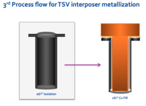 Alchimer’s wet deposition processes reportedly enables such reduced dimensions because of its ability to coat conformally regardless of via topography or aspect ratio. In fact, its established four-step process flow (isolation, barrier, seed, fill) reportedly achieves 20:1 aspect ratio TSVs. The second process flow combines the seed step with the fill step. I wrote about this technology recently after I interviewed the company’s CTO and VP of engineering, Frederic Raynal and Vincent Mevellec, director of technology, at the European TSV 3D Summit.

Mevellec presented again at IMAPS DPC 2013 with some technology updates to report that promise to further streamline the process and improve cost savings. The company is working toward a two-step process flow with isolation and direct fill, eliminating the need for the barrier step.
“We are working with end-users and equipment suppliers to have something at customer sites before the end of year,” said Mevellec. The remaining hurdle, he explained, is obtaining reliability data and electrical test. To achieve this, Alchimer is entering into a JDP with a European R&D center, where “in a few weeks” they will be able to perform full metallization processes and electrical tests. Mellevec said we should be on the lookout for data to be shared in three months or so. Standing by for that …
In his presentation on cost modeling, Chet Palesko, SavanSys Solutions, said that many of the processes discussed here are innately slow and expensive, (specifically he noted temporary bond/debond, deep reactive ion etch (DRIE), traditional dry deposition processes (CVD and PVD) and filling by electroplating) “Some things won’t get any cheaper,” he said. “Anything done in the Fab is more expensive than the same thing done at a PCB facility due to the overhead.” In Palesko’s opinion, its yield that is the ultimate cost driver, and that once yield is driven up everywhere in the flow, process costs will be differentiators. “Do not underestimate the impact of indirect costs,” he explained. “Margin and risk factor cost can swamp direct costs.”
However, after listening to all of these speakers, I’m likely to check the “all-of-the-above” box on the cost reduction question. While as Palesko says, increased yield will likely impact the bottom line most dramatically, chipping away at process costs through streamlining steps and adopting promising alternatives may also positively impact cost-of-ownership. It certainly can’t hurt. ~ F.v.T.


