
Yesterday at the pre-conference symposium for 3D Architectures for Semiconductor Integration and Packaging (3D ASIP), I was fortunate to get an up close and personal tutorial preview by David Wang, CEO of ACM Research, on the tool manufacturer’s latest process solution for two critical points in the TSV fabrication process. The first is a TSV clean process that puts a new twist on existing concepts, and the second is a reverse plating process to relieve stress from a plated wafer. Daquan Yu of IME will talk about both of these processes, as well as the tools associated with them, in a presentation today (Thursday, December 13, 2012).
Scrubbing Bubbles
Wang explained the importance of cleaning Through Silicon Vias (TSVs) post etch before the seed layer is applied, to remove any photoresist left behind on the TSV sidewalls, so that the seed and barrier layers will adhere properly. Achieving this is key for high-volume productivity and yield, said Wang.
 Wang explained how ACM has done what no other clean tool manufacturer has been able to do up until now; achieve a consistent clean across the TSV wafer using megasonic energy. While the concept of using a mechanical wave to create microbubbles that oscillate up and down TSVs at megahertz level is nothing new, achieving a consistent clean with it is. “Megasonic energy on a wafer is hard to control, and others have abandoned it because they couldn’t make it work.” He said. “We figured out how to control it across the wafer.”
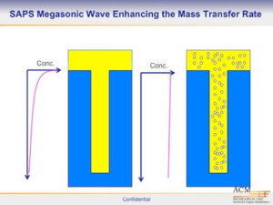
It’s called Space Alternate Phase Shift (SAPS) and here’s how it works:
Because wafers aren’t uniform, with most having a certain percentage of warpage, it’s impossible to maintain a consistent energy gap between the wafer and the megasonic device that delivers the mechanical wave. While other companies kept trying to bring Mohammed to the mountain, Wang’s team realized that to achieve the necessary performance required bringing the mountain to Mohammed. In other words, rather than trying to address the wafer warpage to solve the problem, ACM looked to the gap for a solution. What they discovered is that if the megasonic device was movable rather than fixed, consistent energy can be maintained across the gap. Each point in the wafer gets the same full cycle of sonic energy dose, which is repeated sequentially until the TSV sidewall surfaces are uniformly clean, standing ready for barrier、seed and electrical chemical deposition (ECD).
Old Story, New Application
About 10 years ago, and clearly before its time, ACM Research introduced a reverse electroplating process using an electrolyte bath and a charge to remove copper ions; and subsequently copper metal that dissolve into the electrolyte. Now with the advent of 3D ICs, its time has come.
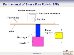
Wang described this process as “stress free polishing”; addressing a particularly critical challenge for 3D ICs. Essentially, what it does is to decrease stress build-up from plating TSVs by removing the bulk of the copper plating layer from the TSV wafer post via fill.
This stress-free “polishing” requires neither pad nor touching the wafer. The step is added after ECD and prior to anneal, reducing the stress created during the anneal step. “SFP releases stress because it removes film from the wafer and reduces copper thickness by 90%,” explained Wang. “We can take a plated wafer that isn’t uniform and can create uniformity in the SFP process through adaptive control.” This means that current is adjusted based on the thickness of the copper layer. SFP isn’t performed in lieu of chemical mechanical planarization (CMP), rather it is an added step performed after the ECD process, followed by the anneal step, and subsequently required a much reduced CMP step.

In addition to developing both these processes, ACM has built the tools to perform them. Both are HVM-ready, module-based systems that can be implemented in the R&D environment and then expanded as needed to HVM by adding more modules. The SAPS stand-alone tool is available in configurations of 2, 4, 6 and 8 modules.The SFP tool includes traditional clean chambers along side the reverse electroplating.
One might think adding an additional process step means more time and more money, but in the case of SFP, the opposite is true. If you can deplete your copper by 90% through SFP, you can increase your CMP throughput, reduce the number of CMP tools needed, and reduce the use of CMP slurry; all of which helps lower the cost of 3D ICs.
While the company isn’t new to the industry, this is their first foray into the 3D IC market, and after seeing what the company has to offer; I’d say they’re a welcome arrival on the scene. ~ F.v.T.


