
It wasn’t on the final agenda, but thanks to a last-minute presentation switch by BiTS Workshop keynoter Jim Feldhan, president of Phoenix-based Semico Research, 3D became a featured topic at this year’s event. For the past few years, BiTS General Chair, Fred Taber, has contracted me to conduct video interviews at the event for the BiTS Workshop website. The fact that I had the opportunity to get another analyst’s perspective on 3D was a bonus.
“3D is sexy, but it’s still going through puberty. We expect the technology to be adopted faster than it is,” noted Feldhan, adding that for 5 years we’ve been hearing that 3D will be adopted in two years. He says the hold-up is largely due to gating issues such as the ecosystem, EDA tools, assembly and test processes, and product life and reliability testing. Up until 2012, there have been reliable and low cost solutions in traditional single die packages, and system-in-package with stacked die. However, the performance improvements from 2.5D interposer and 3D TSV devices will make them vital to memory in 2012 and memory + logic in 2014.
Addressing the question of whether 2.5D interposers are a stepping stone to 3D, Feldhan said no. He believes it will be a stand-alone technology because it’s cheaper, and is likely to be adequate for many applications. He says he sees opportunities for large pitch interposers for MEMS, RF and high performance systems. Currently, TSMC is the main supplier of leading-edge interposers, and cost is double that of a 300mm wafer. He expects some healthy competition will bring that cost down, and said GlobalFoundries, UMC, Samsung, and IBM all have plans to enter the market.
According to Feldhan, 2012 will see pilot production for 3D DRAM with high volume manufacturing (HVM) coming in 2013. The hybrid memory cube (HMC) of DRAM on logic will be in pilot production in 2013, with HVM in 2014. 3D NAND will also be in pilot production in 2013 and HVM in 2014. From an applications perspective, the first to adopt 3D will likely be data centers and base stations, where the 10x performance at lower power consumption benefits offsets the cost of implementation. Consumer products will follow as indicated below (Figure 1).

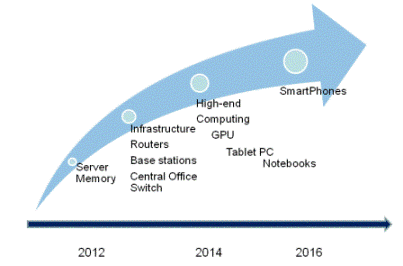 Figure 1: Interposer & 3D TSV IC Application Roadmap, (courtesy of Semico Research)
By 2015, he expects market penetration for 3D devices in servers will be over 60%. “But when it comes to tablets and smartphones, how quickly we can get the price down will dictate how they will penetrate the market,” says Feldhan. In smartphones, he says with 3D, smart phones can achieve 10X and 4X the battery life vs. traditional PCB/IC assembly. However, the semiconductor bill of materials costs must be reduced to between $100 and $125 for tablets, and $80-100 for smart phones. Market penetration for 3D devices for tablets and smartphones is expected to reach just over 10% by 2015. Ultimately, Feldhan says the bottom line as seen by Semico Research is this: applications need performance that can be provided by 3D. Adoption is starting, but the eco system still needs development & maturity. Therefore, implementation will occur in stages and cost reduction is the Holy Grail. ~ F.v.T.


