
A few weeks ago, I came across an article on a new nanotechnology process in development at Rice University that can be used to build transparent, flexible 3D memory chips. According to the article, these chips could replace flash memory in thumb drives, smart phones and computers. The transparency also makes it perfect for touchscreen displays, and such futuristic concepts as smart glass for windshields that could then have functionality built into something that previously just served the purpose of optics. Really, the possibilities appear to be endless. Of course, the 3D aspect of the technology is what caught my eye, so I contacted James Tour, Ph.D, the synthetic organic chemist at Rice who is
responsible for this technology, to get more details such as how these chips are manufactured, how far along in the development it is, and how it measures up cost-wise to current technologies – stuff like that.
What makes it 3D?
First of all – I wanted to clarify the 3D nature of this technology to properly classify it among the ever-growing species of 3D integration processes. Tour explained that the technology itself is not a 3D structure, but that it lends itself to on-chip 3D configuration (not to be confused with chip-to-chip stacking). So if you’re looking for another example of monolithic 3D, this is it.
This memory device does not rely on transistors, but is based on resistive memory rather than a stored charge. As a result, it only requires two terminals – a source and a drain–to function, and that is what makes it more amenable to 3D. Ultimately, it’s a build-up process using silicon dioxide in which multiple memory bits can be stacked on chip at each crosspoint. Silicon nanofilaments within the oxide create the on/off states. “It’s a very simple solution,” noted Tour. “The memory is inherently formed by putting voltage to the chip. Depending on the voltage applied, the memory can be switched off, and on, and really, really on.” He added that silicon dioxide is a very friendly material and can be used with different wiring such as silicon, tungsten, and copper. The advantages over current Flash memories, which Tour says can only scale so far and will run out of room in 6 or 7 years, is its seemingly limitless scaling ability. “With flash, you could never aggressively scale this small. The nanofilaments are <5nm,” noted Tour. “This technology can go much further than where Flash can take you.” He added that this type of memory can be written, erased and rewritten, unlike the one-write only 3D memories on the market today.
How is it Constructed?
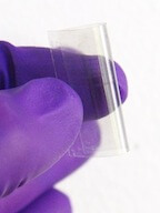
Another bonus that could help bring these chips online sooner than later, is they can be built using standard CMOS processes and tools, and therefore requires no changes to the existing infrastructure. Additionally, Tour says it’s not an expensive process and the materials involved are really fairly cheap. Beginning with a silicon wafer as a substrate, the electrode 1 (source) layer is constructed, followed by the deposition of a silicon oxide layer, and then electrode 2 (drain) is the final layer. These layers can be repeated to create a 3D structure. The same can be done using a plastic or glass substrate. In fact, a working two-terminal memory device that can be stacked in a 3D configuration and attached to a flexible substrate was developed in the Rice Lab by Tour, along with faculty collaborators, Professors D. Natelson and L. Zhong, and assisted by Jun Yao, Ph.D, and Jian Lin, Ph.D. Transparent electrodes such as indium tin oxide must be used to make it transparent for use in displays. Alternatively, graphene electrodes, which are conductive, flexible and transparent, can be used to make flexible memory (see figure).

Can it be integrated with Logic?
As memory on logic is a major topic these days, I asked Tour how the memory can be integrated with logic die. While it hasn’t been tried yet, Tour is confident that it can be done. “It’s a given that you integrate logic with memory,” he said. “You could start with a 2D logic chip and wire a 3D memory on top of it. Or you could start with the memory and put the logic on top, but the concept hasn’t been tried yet.”
Target Applications
I already mentioned possible target applications in the consumer space (smartphones, computers, touchscreen displays), but the primary applications will likely be in the military and aerospace markets due to its resistance to heat and radiation hardness. Tour says these chips can withstand extreme temperatures of 600°C, hostile conditions, and demonstrates radiation hardness that doesn’t get knocked out by X-ray, proton or heavy ion irradiation, making them ideal for use in satellites and systems that need to be resilient in space, or for the military during nuclear conflict. “We’ve built working demos in the lab, and now we’re sending it to the International Space Station to see how it does up there,.” he said.
While Tour thinks ramp to production wouldn’t take long, because the infrastructure is in place, there’s no denying this technology in still in its infancy. “We’ve done the research step, but there’s a huge ‘D’ in R&D.” noted Tour. There is currently a paper under review that Tour expects will be published in the next 3 months. Hopefully this will generate enough interest to fund future development. Tour already has seen interest from major flash memory manufactures who know they will need a solution for future scaling sooner than later. As Tour succinctly stated, “If you’re not in the 3D memory space within 4 years you’re not in the memory business”. So who knows, in a few years you might be wearing a transparent smartphone on your wrist that contains one of these 3D flexible memory devices. ~F.v.T.


