
In addition to my Monday blog post, there has been a plethora of articles authored by other industry bloggers about the 3D Friday event, most of them focused on the user perspective, as well as the panel. I haven’t seen a whole lot of attention paid to the vendors, Mentor, Cadence and Synopsys – all who had some input on their company’s offerings and readiness for 3D IC so far. So I will give them some air-time here.
Design for Test
Steve Pateras, of Mentor Graphics, kicked off the vendor portion of the presentations with a look at design for test (DfT) solutions and in particular, built-in-self-test (BIST). Among the challenges for what he called a generic 3D stack, where SOCs and or ASICS are stacked together with interposers and memory stacks, how do you ensure that what you’re stacking is good? And it’s not just about testing known good die (KGD) to start and a final package test at the end. When you’re dealing with 3D stacks, you need to conduct tests all along the way. Additionally, Pateras explained that the main form of stacking is wafer-to-wafer (W2W), but it only works with homogenous die and it’s difficult to control stack yield. On the other hand, although a much slower process, die-to-wafer (D2W) stacking allows for heterogeneous stacking, and stack yield is controlled with KGD and partial stack test. So to really take advantage of W2W, there’s a need for comprehensive wafer test coverage.
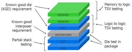
Overall, Pateras test challenge list included:
- A KGD requirement
- A known good interposer requirement
- Partial stack testing
- Memory to logic testing (where the memory stack meets the logic chip)
- Logic to logic testing (with logic chips on either side of the interposer)
- Die test within the package
Luckily, according to Pateras, there are many solutions available that were originally developed for the 2D world, and particularly from the early configurations of 3D packaging that had similar challenges minus the through silicon via (TSV) element. BIST is one such solution, and he focused most of his presentation on evolving BIST solutions for 3D IC. “BIST has a special place in that space,” explained Pateras. “It is embedded by nature and has the ability to be re-used.”
TSVs can come in handy for BIST, providing access within the stack that’s not possible with wire bond. Pateras said only a few dedicated TSVs can be used to route test data up and down the stack. The challenge, he noted, is standardization. If all the chips that are being stacked were designed with one EDA vendor’s proprietary tool, than you’re fine. But if the die being stacked comes from different vendors, they need to be able to “talk to each other.” What’s needed, therefore, is a standard architecture to support heterogeneous die from multiple vendors.
Pateras says BIST is best suited for re-testing die within a stack. He also outlined ways it can be used for stacked memory. Additionally, built in self repair (BISR) has been successfully developed for repairing memory. BISR for TSVs is similar in concept, and is thought to be viable solution once it has been fully developed. So in a nutshell, according to Pateras, BIST solutions will play a key role in 3D test. Existing commercial BIST solutions are directly applicable to 3D, and improvements and new capabilities for 3D are under development.
3D Wrappers
Also reporting on DfT, was Bassilios Petrakis, of Cadence, who examined what it takes to build a complete test flow for 3D ICs. He began by noting that 3D stacking of ICs is a hot DfT topic, and focused his presentation on modular testing techniques for 3D IC stacking that Cadence has developed. According to Petrakis, because test access is distinctly different and requires pre bond, mid bond, post bond, and final test, it needs to be modular and involve the core, die and interconnect. Cadence wants to support the 3D IC portion, and has developed a “3D wrapper” to isolate the logic – core test inside it. They’ve also developed tool flow for the automatic insertion of 3D wrappers, and the method can be extended to other interconnect types such as interposers.
In his presentation, Petrakis detailed the DFT architecture, including the 3D wrapper generation flow, and the resulting test chip developed for TSMC, that demonstrated negligible area costs for the wrapper.

Wide I/O DRAM TSV
Marc Greenberg, also of Cadence, took over the podium and turned discussion from DfT to the company’s participation in test chips, focusing on the wildly popular Wide I/O for DRAM. Greenberg talked about a paradigm shift and that at this point if one had to choose there are more pros in the 3DIC TSV side than both SOC and wire bond, and that the con list is disappearing.
The company has been deeply involved in what has been dubbed the “WIOMING” test chip project with ST Ericsson and CEA-Leti. The test chip was designed using a complete Cadence tool flow. As part of this project, Cadence developed a wide I/O DRAM controller with specific solutions to address such challenges as the merging of existing and new technologies, address new test requirements, and verification.
While challenges still remain (thermal issues, ecosystem issues, and cost), Wide I/O and TSV are real, notes Greenberg. With five years of development, conducted in close partnership with foundries and customers, and multiple 3D IC tapeouts under its belt that include 8 test chips and one production chip, Greenberg says Cadence has a proven IC solution ready to go.
Standards are Number 2
Synopsys’ was represented during the panel discussion by Steve Smith, Senior Director 3D-IC Strategy and Marketing. While Smith acknowledged that the 3D ecosyetem is happening, he says its “way more complicated than anything we’ve experienced” because the necessary involvement across the supply chain. Synopsys has historically taken an evolutionary approach to 3D IC, supporting developments in 2.5D interposer technology rather than fully embracing 3D IC. However, late last month the company announced a 3D-IC initiative to accelerate the design of stacked multiple-die. The solution is reportedly available now in beta and is expected to be in production next quarter. According to Smith, Synopsys tools have already been used in 3D design for work in thermal and mechanical stress analysis. Smith’s main message, which was the polar opposite opinion of the rest of the panel, was that while most believe standards are needed before more progress can be made, he believes standards are more likely to evolve as the technology is adopted.
Honestly, with the EDA vendors firmly on board, we’re running out of excuses to keep this from happening. It’s just a matter of time. ~ F.v.T.


