
 |
| View slide show of my visit to NEXX |
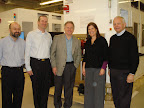
It’s easy to see why NEXX is experiencing growth. It’s all about attitude, and the enthusiasm among NEXX’s team is contagious. I spent yesterday afternoon (Thursday, March 5) visiting the company’s new headquarters in Billerica, MA, meeting with the executive team, and touring the manufacturing facility. The team had lots of exciting news to share, and brought me up to speed on the technology, tools, and what CEO and president Tom Walsh called their “roadmap alignment” for the Stratus line of plating tools.
Strategic Collaborations
NEXX has always seen the benefits of collaboration. For smaller companies in a big pond, it helps to level the playing field and leverage know-how. Senior project manager, Mark Welsh, talked to me about current collaborations with SEMATECH’s 3D Interconnect program and IMEC’s Industrial Affiliation Program (IIAP) on 3D integration. Welsh explained that unlike equipment/supplier programs, which focus on educating IDMs and OSATS on new processes, these joint development programs (JDPs) allow affiliates to learn what the end user’s future requirements will be, and work toward that goal. “The IMECs or SEMATECHs are driving the design of the process flow,” he explained.
In the case of SEMATECH’s program, NEXX will collaborate on developing innovative electrodeposition technology for high-yield, low-cost copper electroplating to enable high-density 3D through-silicon-vias (TSVs). Research with IMEC will focus on joint R&D for TSV metallization and micro-bumping. Both efforts involve the Stratus line.
And there’s more. The team was fairly bursting with news of the latest collaboration that will be announced during IMAPS Device Packaging Symposium this week. All they could tell me at that time was that it involves a major IDM and will really launch the company into the limelight. Trust me, as soon as I know, you’ll know.
Technology Progress
Although not the only technology story to tell, TSVs process developments are at the top of NEXX’s list. Arthur Keigler, V.P. of technology talked to me about the “second phase” of work the company has been doing with the Stratus line to lower the cost-of-ownership. “We’re working on a new module technology that will reduce chemistry consumption for the process,” he said.
Also in testing phases is a process for pre-treatment of wafers prior to filling them for better control of surface chemistry in the vias. The structure of the Stratus Line, which is based on a vertical orientation of the wafer and is modular, is ideally suited to this process because it allows for what Walsh calls a “multiple sequencing capability.” Additionally, with the wafer in a vertical orientation, bubbles are less likely to get trapped in the vias, reducing the possibility of voiding.
The process flow goes like this: The first set of cells perform the conformal plating process for uniform coverage of even hig-aspect ratio vias. In the second cell set, vias are super-filled most of the way, and then the process slows to minimize a possible “mound” effect.
Walsh explained that in the traditional “fountain cell” system, in which cells are horizontal, the process would call for additional cells to be added to the system, changing the footprint of the tool. Alternatively, this multistep solution for TSVs allows for the most wafer-outs in a small footprint. In terms of productivity, this vertical mode is it.
Recent work with Alchimer, whose process and chemistries NEXX has licensed, is focused on copper barrier-on-plate using a wet process. The application that will benefit most from this work is high-aspect ratio vias. Other applications served by NEXX tools and processes include lead-free, UBM for copper pillar bumping, and micro-bumping. In fact, the work with the IDM-who-must-not-be-named will focus on micro-bumping processes.

Roadmap of Alignment
Walsh told me that last year’s focus was on the Stratus. The “Roadmap of Alignment” has included formalizing engineering methodologies to make the Stratus the production-worthy tool-of-choice. They’ve also formalized processes for in-house testing, and have aligned with the needs of suppliers to develop throughput and speed enhancements.;
While much of my visit focused on developments with the Stratus tool, NEXX’s PVD tool family deserves some ink. Although a mature product, there is a subtle roadmap in place for them. The Apollo, lunched last year at SEMICON West, features better particle control, etch uniformity and thin wafer handling. Target applications here include handling wafers as thin as 100µm for applications such as Backside Metal (BSM). Additional handling applications include non-silicon and highly bowed substrates for build-up and eWLB processes.
Business model for success
At the end of the day, success is all about serving the customer. In the 3D space, customers are putting their investments into the development side. “We’re working with them,” says Walsh.“Their motivation is where we want to be.” It’s important, he said, to keep up the enthusiasm.
Part of NEXX’s model, he says, is to support the customers locally. For example, for one major Taiwanese OSAT-who-must-not-be-named, NEXX has a local group, including an applications engineer and a process engineer, in place to provide service and support.
During these times, it’s especially important to provide great service to customers and build relationships,” says Walsh. “Our success model is based on delivering solutions through product, services and support.” The model must be working, because business is hopping at NEXX Systems. – F.v.T


