

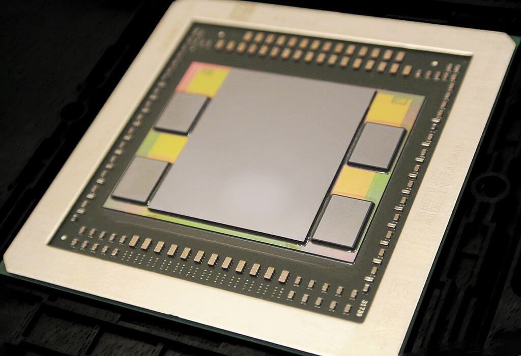
It’s official. Die stacking and interposer integration have been implemented in a high volume consumer application. AMD officially launched the Fiji GPU processor, the first to feature die stacking and high bandwidth (HBM) technology, amidst quite a bit of media fanfare at the E3 gaming conference in Los Angeles and in Beijing on June 16, 2015. This is big, news for the 3D integration community. Really big.
Fiji is the heart of the Radeon™ R9 Fury product family, AMD’s latest line of video graphics cards for high performance, enthusiast gaming. I first saw mention of it in an EE Times post by Rick Merritt, who had interviewed Nvidia’s Jen-Hsun Huang, and linked to a news item by Jessica Lipsky, who was covering E3 gaming conference.

I figured something pretty big was happening, because Bryan Black, Senior AMD Fellow, was scheduled to present during the SEMICON West STS session, Packaging: The Very Big Picture, and he doesn’t generally like to present if he doesn’t have something new to report. He did it in his usual understated style: “We’ve been working on this program for 8 years. I’m excited to be here and tell you that we’re done. It was fun.”
Calvin Cheung, VP of business development, ASE, was a bit more animated when it was his turn to speak about the part ASE played. “WE DID IT! It’s been an incredible journey. Looking back, it’s a small miracle from the first day we engaged to shipping parts.” ASE has been designated as the product integrator, although there have been many other partners companies involved throughout the journey.
“This project required collaboration with 20 different companies and government organizations before delivering the final product,” said Black. “We worked with many partners along the way. Some disappeared, some delivered. Some we’re still working with.” The final product integrates graphics chips from TSMC, OSAT partners ASE and Amkor; HBM was procured from SK Hynix, and UMC provided the interposer.
The Fury/Fiji Story
According to Black, the Radeon™ Fury represents a lot of industry firsts: It’s the first time die stacking is used in the graphics market; it’s the first high volume manufacturing (HVM) interposer with an expected 1M parts to ship soon. “We will ship a tremendous number in the next year and a half,” noted Black. It’s the first time TSVs with micro-bumps are used in the graphics industry, and it’s the first time 22 discrete die manufactured by different companies are integrated into one single package. Talk about a team effort!
Black went on to detail the journey itself, noting that the 8 years of development were followed by 6 months of product ramp from ASIC wafer to volume production. 12 hours from the first sample, the product was booted and playing 3D games, he said.
There were numerous prototyping activities over the years beginning in 2007 with CPU and mechanical DDR3. AMD’s first interposer used large micro-bumps and TSVs. 2012 was a big year because they achieved feasibility with multiple OSATS and foundries and established the process of record (POR) for business models, wafer sort solutions, known good die (KGD) solutions, system and component thermal solutions, and interposer processes. All in all, says Black, 15-16 unique prototypes were built for the program.
“In 2013, we discovered how expensive it was, and we started to focus on costing it down,” said Black. So far, they’ve achieved a 50% cost reduction and there’s lots of room to remove cost.
Cheung reminisced a bit about the early days, and said when ASE first met with AMD in 2010, they thought this project would be “another tombstone on the roadside.” There was no product roadmap in place, no ecosystem or supply chain. They viewed it as a proof of concept program with numerous challenges including CPI, thermal issues, backside thinning processes were risky, as was bonding and assembly. TSV test reliability was still being figured out, as well as failure analysis resources.

“So how did we get here? It was a huge commitment of resources, capex, new process equipment, and technology core competency development,” said Cheung.
Bill Chen, ASE Fellow, further defined ASE’s involvement, explaining that they handled the integration of the GPU and 3D stacks. He also noted that ASE is committed to support AMD in rolling out the entire family of Fury products.
While the Radeon R9 Fury X is the first device and the most complicated in the Fury product family to feature the Fiji GPU with HBM, the company intends it implement it throughout the Fury line. According to Black, next up is the Fury Nano for smaller game towers, followed by 2 Furies on each board.
“The reason AMD is pushing hard and started with the biggest device is because if you build the most complex devices, the rest will be easy,” explained Black.
“I started working on die stacking technology 15 years ago because I think its going to change the world by driving higher performance into smaller form factors,” said Black. “We will see more HBM in more AMD products. We didn’t develop the technology just for this, we developed it for the future. “
“This technology will benefit the semiconductor industry for a long time to come.“ added Cheung.
I told you this was big. ~ F.v.T.


Good to see that the 50 um pitch micro bump flip chip technology that we had developed at Motorola and then put into volume production for Gallium Arsenide Power Amplifiers for Mobile Phones some 20 years ago has finally diffused out to the OSATs, in this case via Bryan who used to be at Moto.
But the throughput ( e,g. for TCB ) is perhaps still too low for volume applications. At APSTL we are once again looking at TCB to raise the throughput beyond about 1000 uph that we were getting with FC – TCB bonders of custom design back in 1994