
Samsung continued their 3D NAND march with an impressive presentation at the 2015 IEEE International Solid-State Circuits Conference (ISSCC) in San Francisco on February 24th. Their presentation, “A 128Gb 3b/cell V-NAND Flash Memory with 1Gb/s I/O Rate”, listed only 34 authors this time compared to 46 last year.
Remember that Samsung is the only company so far to have 3D NAND products and peer-reviewed presentations. They certainly give the impression of being far ahead of their rivals. Analysis of this, their latest presentation, gives a clue of what they need to do next to maintain the momentum.
Metaphorically, base camp has been set up, climbing ropes and crampons have been cleaned and laid out neatly, oxygen masks have been made ready. Mount Everest beckons. The only way left is up.
But before we look into that, let me begin by summarizing the facts as given in the presentation.
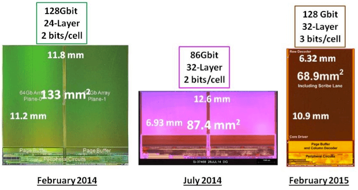
- 128 Gbit single chip.
- Die size is 69.9 mm².
- 32 active cell layers.
- 3 electrical bits per physical cell.
- Charge Trap Flash based.
- Endurance of “over 5K” program/erase cycles.
- 2 bitlines in a channel hole pitch
This is certainly much more aggressive in both die size and stack height compared to their 2014 ISSCC presentation. Interestingly, it is also a more aggressive die size compared to their 32-layer product chip introduced around mid 2014. That was 87.4 mm², 2 electrical bits per cell and 1 bitline in a channel hole pitch for an 86 Gbit die.
The figure shows the progression in Samsung’s product chips.
We can work out the following details too.
- Die dimensions are ~ 6.32mm by ~ 10.9mm.
- Array efficiency is ~ 72%.
- Physical cell size on each layer is ~ 36200nm².
- 1 Tbit will need 256 active cells in a vertical NAND string.
The first thing to notice is the physical cell size, which remains larger than 30000 nm². This hasn’t changed by much since my first estimate from a year ago. In fact, it is still about 27 times the physical cell size of Micron’s 16nm 2D NAND. Although Toshiba and Sandisk had a 2D NAND presentation at the 2015 ISSCC entitled “A Low-Power 64Gb MLC NAND-Flash Memory in 15 nm CMOS Technology”, no physical cell size was given to be able to compare with.
The second important point is that Samsung has managed to economize on the amount of periphery circuitry needed to drive the memory. Here, they used about 19 mm² of CMOS silicon whereas they needed about 27 mm² a year ago for their 24-layer.
And of course the third point is the use of 3 bits/cell while last year they had 2.

As I explained in my recent 2015 outlook, the 3D NAND manufacturers have three main paths to lower cost per bit, namely multiple electrical bits per cell; longer (more stacked layers) strings; and lateral shrinking of the cells. Another path with less leverage is economizing on the peripheral circuitry.
It looks like Samsung has done the first along with the peripheral circuitry reduction. I also heard that they may be looking at extending the first to 4 bits/cell. These optimizations, although admirable and not straightforward, pale in comparison to what they need to do now.
Extending the mountaineering analogy, they have scaled Ben Nevis, the highest mountain in Scotland, and now are preparing to climb Mount Everest.
To double the existing chip capacity from 128 Gbit to 256 Gbit, all vertical channel NAND strings will need to lengthen from 32 cells to 64 cells. Besides the vanishing string current in non-crystalline channels that such lengthening entails, each cell will also experience more disturb which may affect the ability to use 3 bits/cell.
In addition to the dying string current, the channel hole and source trench taper angles must remain within a few tenths of a degree from the normal all the way up. Otherwise, the whole edifice can be undercut in cost by other approaches. And remember, to get to 1 Tbit on a single chip from where they are now will mean vertical strings of 256 cells, each with 3 bits/cell. Hearty congratulations to Samsung for again an amazing achievement.
But do I see a swallow optimized for graceful gliding? Or is this a peacock with a dazzling tail? For the moment, I’ll stick with the latter. ~ AJW