As the industry pushes toward ever-greater levels of semiconductor performance, integration and efficiency, the promise of 3D integrated circuits (3D ICs) stands out as a true game-changer. By stacking dies and embracing heterogeneous integration, 3D ICs make it possible to create compact, power-efficient systems far beyond what can be achieved with conventional planar designs. However, this leap forward also creates new—not just incremental—verification challenges that are stretching traditional methods to their limits.
Ensuring that these innovative devices deliver robust, reliable performance demands a fundamentally new approach to physical verification—one that unifies all relevant physics domains, enables system-level collaboration, and drives efficiency throughout the entire design and sign-off process.
The ROI of fully integrated multiphysics verification
For decades, physical verification of integrated circuits largely meant applying design rule checking (DRC) and layout versus schematic (LVS) to ensure manufacturability and electrical correctness of a single-die device. As device complexity, performance and power requirements all ramp up, these foundations are no longer sufficient—especially in the world of 3D ICs, where the boundary between electrical, thermal and mechanical domains has disappeared.
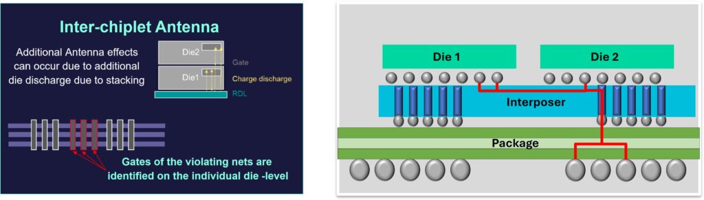
A system that includes multiple stacked dies, through-silicon vias (TSVs), redistribution layers and advanced packaging creates new interactions and risks that no one discipline can fully catch in isolation. Mechanical stress induced by die stacking or thermal expansion mismatches, for instance, can introduce warpage and alter device behavior at the transistor level. Elevated power densities and vertical current paths compound risk for electromigration (EM) and IR drop failures. Even fundamental checks like DRC and LVS must operate in a world where connectivity now exists both laterally and vertically, and failure to account for these complexities can threaten yield and reliability.
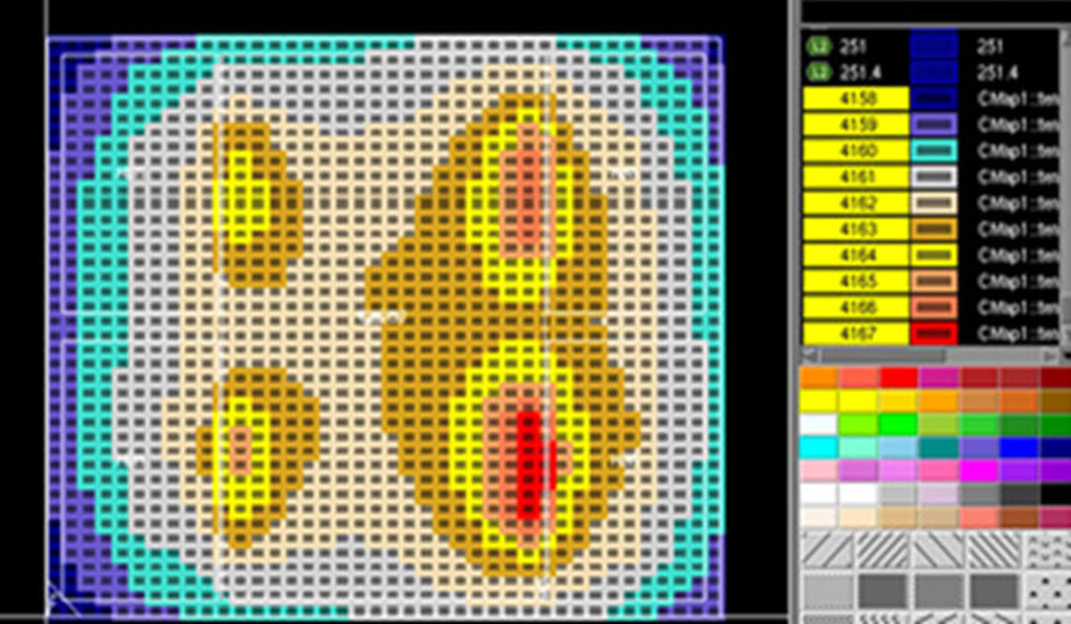
That’s why our approach is to enable fully integrated, sign-off ready multiphysics analysis, supporting not only DRC and LVS, but also system-wide antenna analysis (figure 1), full-stack EM/IR checking, advanced thermal and mechanical stress simulation, and more—within a single, automated verification flow. Running these checks in parallel, with robust data management and automation, delivers several key ROI benefits:
- Faster convergence: Early, concurrent simulation across the relevant physical domains reveals true root causes, enabling targeted solutions instead of over-conservative design.
- Reduced design risk: Integrated sign-off means fewer late-stage surprises and less manual rework, ensuring that failures are caught at the right time by the right team.
- Accelerated time to market: Efficient workflows and seamless data management minimize bottlenecks, supporting global, cross-functional design efforts.
Bridging technical complexity: automation and collaboration in the 3D era
System-level multiphysics verification is essential, but practical success requires not only powerful tools but also equally robust approaches to data management and collaboration. As 3D ICs bring together more dies, interposers, packaging elements and design domains, no isolated team can ensure success alone. Reliable sign-off depends on real-time information flow between design, verification and manufacturing—in effect, creating a digital thread that connects every stage and stakeholder.
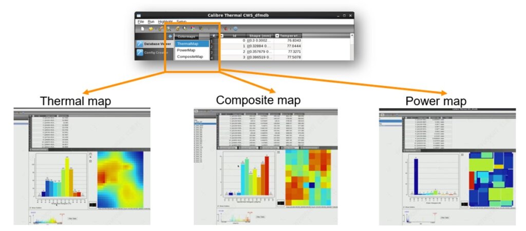
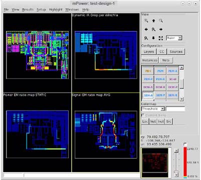
Our methodology starts with creating comprehensive models of the device—the electrical activity (represented by accurate, tiled power maps), power dissipation and material properties that affect heat flow or mechanical response. Early in the cycle, these models can be created from layout data or using industry-standard estimation tools, then refined as the design matures and more detailed data is available. Figure 2 shows temperature results and power maps for die-level thermal analysis.
Seamless integration between physical design, packaging, and system-level teams is critical. Advanced stress analysis—once confined to late-stage package teams—can now be performed at the transistor or block level, directly by design engineers. Layout data and material maps are fed into a custom solver, providing early feedback on die warpage or hotspot risk, and informing block placement or package decisions before costly fixes become necessary.
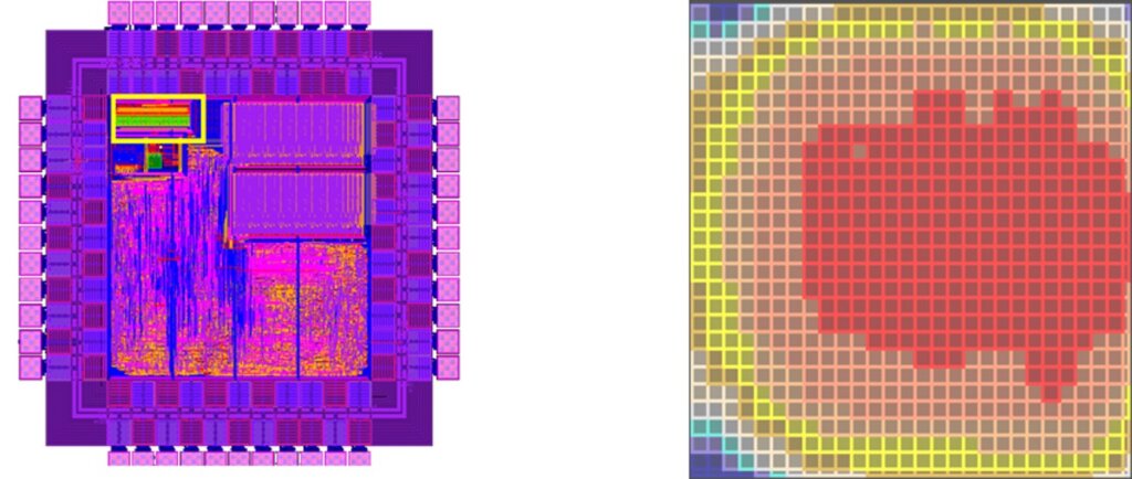
Electrical integrity cannot be left behind. With 3D architectures, electromagnetic and IR drop challenges multiply, as current flows in three dimensions. Dedicated flows for EM/IR analysis, synchronized with the rest of the verification stack, allow teams to identify signal and power path hotspots, optimize routing resources, and validate power delivery from die-to-package to interposer—simultaneously.

Managing this wealth of heterogeneous data across platforms, teams and geographies can be overwhelming, which is why automation and shared visualization are essential parts of our workflow. Hierarchical data processing, process-specific rule decks, and automated reporting streamline the entire process, reducing human error and making complex verification tasks consistent and repeatable. Shared debug sessions, cross-probing and results export further enable real-time, cross-disciplinary collaboration—helping to bridge the gap between layout, packaging, and verification engineers worldwide.
Looking ahead: enabling first-pass silicon success for next-generation ICs
If there is a single takeaway from the emerging world of 3D ICs, it is that old silos—between physics domains, teams, or tools—are no longer sustainable. Achieving both progress and reliability at scale requires a new philosophy: physical verification that is unified, collaborative and comprehensive from day one.
By integrating DRC, LVS, thermal and stress simulation, EM/IR analysis, and system-level automation, we are bridging the complexity gulf and enabling teams to deliver reliable, high-performance silicon—swiftly and with confidence. This comprehensive, multiphysics-first approach not only manages new technical risks, but delivers compelling ROI through earlier closure, reduced design iteration, and improved manufacturing outcomes. In the rapidly evolving landscape of semiconductor design, these advantages will define the leaders of tomorrow.