Although the idea of chiplets has been around for a little while, broad industry interest around the technology really took off around 2018, when AMD released its second generation EPYC processors. Since then, Google searches for chiplets have skyrocketed, and the advanced packaging industry is beginning to seriously consider chiplets as a viable solution to cost, scalability, and flexibility challenges posed by standard system on chips (SoCs).
To provide some quick context, chiplets are small integrated circuits that can be combined with other chiplets to create more customizable and complex SoCs. They offer the freedom to spend money on areas where more advanced technology is needed, while saving money where it’s not.
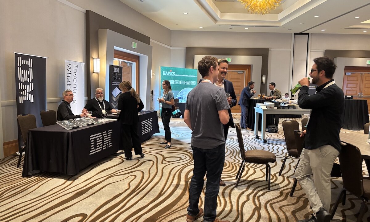
So, to address the uptick in chiplet interest, IMAPS established its CHIPcon conference and exposition. From July 7-10 in San Jose, California, chiplets took center stage. With roughly 180 attendees and 17 exhibitors, this hyper-focused conference touched on everything from AI inferencing and chiplet cost considerations, to standardization, ownership, and more.
If you didn’t get a chance to attend, here’s what you missed.
AI Inferencing and Training is a Primary Chiplet Market Driver
Because much of the interest in chiplets is driven by AI, it’s important to understand where AI stands today, and where it’s headed in the near-term future.
Last Tuesday, Mario Morales from IDC explained that the industry could reach $1 trillion in annual industry revenue by as early as 2028 – two years sooner than the general industry consensus of 2030. AI inferencing, he said, is playing a larger role in overall industry spending.
To meet demand for inferencing, the industry must strategically place chiplets and optimize interconnects to reduce the distance that data needs to travel.
Ashkan Seyedi from NVIDIA addressed this topic in his Thursday keynote. Although he noted that interconnects are not the most power-hungry component of AI inferencing systems, the industry is still incentivized to scale them. This is because moving data is expensive, and there’s a need to manage latency expectations.
For example, optical interconnects provide lower latency and reduced power consumption over electrical interconnects, but scaling optics requires a large number of connections from the servers. This poses its own challenges, and on top of that, optical interconnects are also expensive.
“You pay dearly for every optical pin in the switch, so you have to use them,” said Seyedi.
In favor of shortening communication distances, one solution Seyedi offered is to reduce data center switches and replace them with co-packaged optics. But even though co-packaged optics can lead to significant power savings, the tradeoff is more complicated substrate design and new thermal failure points that may reduce device reliability.
In short, innovative packaging techniques like closely-placed chiplets and co-packaged optics can help scale AI inferencing, but they can also introduce more complexity.
Partnerships and Standardization Are Becoming More Important for Chiplet Enablement
As the industry considers chiplet architectures to address the needs of the AI market, getting ahead of new failure models is driving the need for stronger industry partnerships. This is especially true when it comes to testing.
During the Wednesday, July 9 panel discussion on chiplet ecosystem enablement, Nitza Basoco from Teradyne emphasized the importance of test strategy alignment for chiplets and visibility into who’s responsible for which problems. This can be challenging when companies are unwilling to share their data, but fortunately, this seems to be shifting through models like NHanced Semiconductors Foundry 2.0.
While partners will still expect ROI for offering information, data sharing is proving essential for problem solving the industry’s way toward broader adoption of chiplets.

Standardization was also a key discussion point throughout the event. While having the freedom to customize is a key advantage of chiplets, Kevin Yee from Samsung highlighted that today’s unlimited customization options may be too much. Like Basoco also noted, too much freedom means no one owns problems. It also means that the industry is forced to define custom processes for each customer’s requirements, which can be impractical at-scale.
Because of this, Yee noted that some companies are starting to return to proprietary die-to-die solutions. He also mentioned that some companies have managed to put high bandwidth memory (HBM) into standard packages to further cut costs, although this may not work for higher-end applications.
Finally, the industry will also need to standardize temperature control and whether to classify chiplet assembly as an assembly or a fab process. To address this, drafting new SEMI Standards for chiplets will likely be the most viable path forward.
Chiplet Cost Considerations – Are They Worth It?
One of the primary benefits of chiplets over standard SoCs is that they can offer more functionality at a lower cost. However, depending on the application, this might not be the case. Amy Lujan, president of SavanSys LLC, put it simply.
“Chiplets help reduce silicon cost, but they increase packaging cost,” she said. “You never know if you need to disaggregate until you run the numbers.”
Lujan’s Monday evening professional development course further detailed the ins and outs of chiplet costs. She noted that hybrid bonding is gaining prominence for chiplets because of its quick ability to pick and place die; however, because hybrid bonding is primarily done at a fab instead of an OSAT, it can be much more expensive than mass reflow bonding.
At the end of the day, every design decision impacts cost, performance, and even the broader supply chain. For example, the more complex a chiplet structure is, the fewer suppliers there will be to accommodate the entire assembly and test process. This can result in chiplets traveling around the world from facility to facility, which further increases cost and risk of damage and failure. And as touched on previously, assigning responsibility for chiplet failure is difficult when companies are reluctant to share data with one another.
So, while chiplet manufacturing costs aren’t always ideal, all advanced packaging structures come with cost burdens, design limitations, and complexities. Because of this, the application itself is likely to determine whether a chiplet architecture, fan-out architecture, or another option is best.
Key Takeaways
While the general industry sentiment toward chiplets seems to be warming up slowly, several major challenges must still be addressed before mass adoption is possible. Of everything discussed at this year’s CHIPcon, standardization seemed to be the most urgent. When new packaging structures start making their way into the market, new failures arise as well. Because chiplets are disaggregated, there’s an immanent need for the industry to form partnerships to own failures and find solutions. In addition, new testing methods will likely need to be developed.
Cost is often highlighted as a benefit of chiplets, but this isn’t always true. Instead, the overall cost of a package is largely application specific. From attending the conference, the general group consensus still seemed to favor using established legacy technologies whenever possible, unless chiplets are the only path forward.
To me, the biggest benefit of chiplets seems to be their ability to shorten the interconnect distance between components. This is proving essential for AI inferencing, which is currently the biggest sector driving the industry toward its $1 trillion industry revenue benchmark. Although there are other ways to achieve shorter communication distances that don’t rely on chiplet architectures, chiplets do offer promise over SoCs in this respect.
Personally, I don’t see chiplets becoming a mainstream advanced packaging approach anytime soon, but they do offer a more flexible approach that could be beneficial for specific use cases.