


Packaging Apple’s A20 chip
Apple’s A20 chip is forthcoming; set to power the iPhone 18 and iPhone 18 Pro models in 2026. This will mark Apple’s first use of TSMC’s 2nm process, a step forward from the 3nm processes (N3B, N3E, and N3P) used in the A17, A18, and A19 chips.
TSMC’s 2nm node employs Gate-All-Around (GAA) transistor architecture, which reportedly results in up to 15% faster performance and 30% better power efficiency compared to the A19 chip in the iPhone 17 series. For users, this claims to result in faster app launches, better gaming, enhanced photography and extended battery life.
Apple is also set to adopt what’s being called Wafer-Level Multi-Chip Module (WMCM) packaging for its iPhone processors. WMCM packaging is described as an advanced technology developed by TSMC that enables multiple chip components, such as the CPU, GPU, RAM, and other necessary elements, to be integrated directly onto a single wafer without the need for a separate silicon interposer. This contrasts with older methods like Integrated Fan-Out (InFo), which typically focused on single-die integration. WMCM enables more flexibility in combining different components while maintaining a small footprint. This shift will allow Apple to create more powerful and efficient chip designs, potentially improving performance, thermal management, and battery life.
I know IFTLE readers want to see this package cross section…so do I, but as of yet I have not found such info in public release.
What is reported is that the A20 will be “…physically closer to its onboard memory, enabling better performance and potentially lower power consumption for tasks like AI processing and high-end gaming”.
Apple adopting WMCM packaging means it is moving away from InFo packaging. WMCM is reportedly being developed at TSMC’s Zhunan plant with its Longtan plant also reportedly conducting small-scale trial production. The company is reportedly establishing a dedicated WMCM production line at its AP7, leveraging equipment and process similar to CoWoS-L. TSMC is preparing capacity of up to 50K per month by end of 2026 and estimate the capacity to reach 120K per month by end of 2027.
Intel Upgrades Chip Packaging for Bigger AI
At the 75th IEEE Electronic Components and Packaging Technology Conference, Intel unveiled that it is developing new chip packaging technology that will allow for bigger processors for AI.
While using an organic laminate package substrate to interconnect the silicon dies is the most affordable option, silicon substrates allow you to make more dense connections.
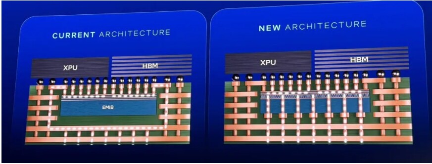
Intel’s EMIB solution, introduced more than five years ago, involves embedding a small slice of silicon in the laminate package beneath the adjoining edges of the silicon dies. That slice of silicon contains fine interconnects that increase the density of connections beyond what the laminate substrate can handle.
Intel also unveiled EMIB-T (EMIB-TSV). In addition to the usual fine horizontal interconnects, EMIB-T provides relatively thick vertical copper TSVs. The TSVs allow power from the circuit-board below to directly connect to the chips above instead of having to route around the EMIB, reducing power lost by the longer connection. Additionally, EMIB-T contains a copper grid that acts as a ground plane to reduce noise in the power delivered due to process cores and other circuits suddenly ramping up their workloads.
It supports high-bandwidth interfaces like HBM4 and UCIe.

All three major EDA powerhouses are working closely with Intel Foundry to develop advanced packaging workflows for EMIB-T.
Cadence’s solution helps streamline the integration of complex multi-chiplet architectures.
Siemens EDA has announced the certification of a TSV-based reference workflow for EMIB-T. It supports detailed implementations and thermal analysis of the die, EMIB-T and package substrate, signal and power integrity analysis, and package assembly design kit (PADK)-driven verification.
Synopsys is also collaborating with Intel Foundry to develop an EDA workflow for EMIB-T advanced packaging technology using its 3DIC Compiler. In addition to the EDA trio, Intel Foundry has engaged other players for EMIB-T support. For instance, Keysight EDA is working closely with Intel Foundry to bolster the chiplet interoperability ecosystem.
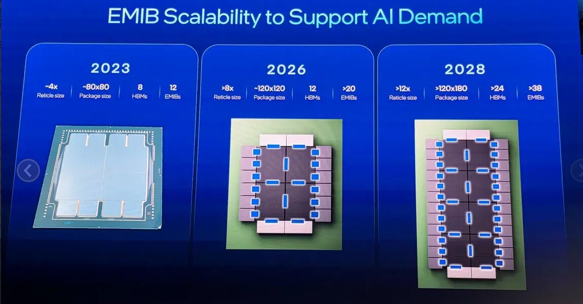
Intel offered the following roadmap showing how they plan to scale EMIB to meet AI demands.
For all the latest on Advanced Packaging stay linked to IFTLE……………………….


