Why the takeover interest in BESI reflects a broader transformation in semiconductor equipment
Step by step, this industry is coalescing around a central battleground. As front-end and back-end technologies converge, control over key interconnect steps is emerging as a critical differentiator. In today’s article, Gabriela Pereira, Senior Technology & Market Analyst, Semiconductor Packaging, and Vishal Saroha, Technology & Market Analyst, Semiconductor Equipment at Yole Group, highlight BESI’s strategic positioning and its broader transformation of the semiconductor equipment landscape.
This growing attention reflects a deeper shift: advanced packaging is no longer a secondary back-end activity. It is becoming one of the most strategic layers in the semiconductor value chain, directly tied to performance, system integration, and future device architectures.
BESI’s March 2026 investor presentation highlights this position. Die attach still represented around 80% of its 2025 revenue, while the company continues to expand in hybrid bonding. With more than 150 cumulative orders, 18 customers, and initial integrated production lines already deployed, BESI demonstrates both commercial traction and technological maturity. Its latest prototype, delivering 50nm accuracy with higher throughput, further reinforces its roadmap toward next-generation interconnect solutions.
Advanced interconnect: from assembly step to performance driver
In advanced packaging, interconnect technologies are no longer simple assembly steps; they are becoming critical performance enablers. Technologies such as thermocompression bonding (TCB), hybrid bonding, and next-generation flip-chips are essential to enabling 2.5D and 3D integration. These approaches support high-growth applications, including high-bandwidth memory (HBM), chiplet-based architectures, co-packaged optics, and AI processors.
Within hybrid bonding, wafer-to-wafer (W2W) approaches currently dominate, but die-to-wafer (D2W) is emerging as a high-growth segment. Estimated at approximately $275 million in 2025, the D2W hybrid bonding market is expected to grow at a CAGR of 57% through 2030, exceeding $2.4 billion.
While early adoption has been driven by chiplet integration, followed by optical engines, broader use in datacenter processors and HBM stacks is expected in the coming years.
A rapidly expanding packaging equipment market
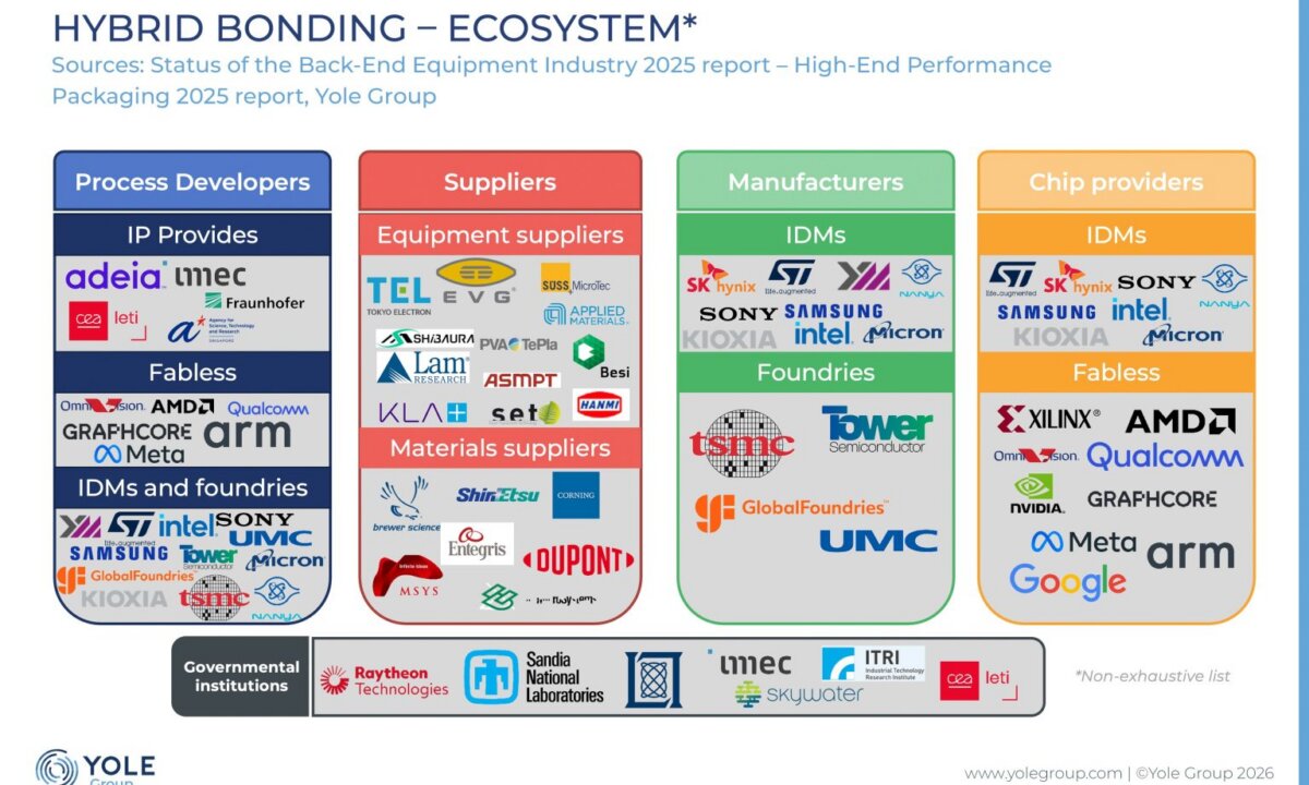
According to Yole Group, the back-end equipment market (excluding services) exceeded $7 billion in 2025. Within this segment, die attach has become one of the most strategic areas, driven by the increasing complexity of interconnects. TCB equipment alone accounted for more than $750 million, while hybrid bonding equipment accounted for more than $150 million, highlighting where high-value investments are concentrated.
More broadly, the packaging equipment landscape is undergoing a structural transformation.
In 2024, front-end-related packaging equipment spending surpassed traditional back-end assembly for the first time, a trend that continued into 2025. Today, front-end packaging equipment accounts for in excess of $8 billion, compared to more than $7 billion for back-end equipment, bringing the total packaging equipment market to above $15 billion.
This evolution reflects a growing convergence between front-end and back-end technologies. Advanced packaging now integrates processes such as lithography, deposition, etch, cleaning, metrology, wafer bonding, and die attach within unified process flows. Developments in wafer-level packaging, TSVs, and chiplet integration are blurring traditional boundaries and pushing equipment suppliers toward more integrated solutions.
Strategic implications for equipment players
In this context, BESI’s positioning makes it a strategically significant asset. Any potential consolidation involving major equipment players reflects broader industry dynamics rather than purely company-level considerations.
Applied Materials (AMAT) is already closely connected to BESI through its 9% stake and its collaboration on the Kinex platform, a fully integrated D2W hybrid-bonding solution approaching high-volume manufacturing readiness. A deeper integration would give AMAT direct control over a key interconnect step, strengthening its position across the expanding packaging value chain.
Lam Research could also benefit from such a move by complementing its upstream process strengths with bonding capabilities. ASML, while less directly aligned operationally, remains a credible strategic player given Europe’s interest in maintaining semiconductor capabilities and the growing importance of precision alignment in advanced packaging. Although less obvious, ASM International has also identified advanced packaging as a growth opportunity, making BESI a potential accelerator in this domain.
An increasingly competitive landscape
BESI operates within a dynamic and expanding competitive environment. Companies such as Hanmi have established strong positions in TCB, particularly in HBM applications. ASMPT remains a major competitor across back-end assembly, while Kulicke & Soffa (K&S) continues to leverage its legacy in wire bonding and die bonding while expanding into advanced interconnect solutions. Additional players, including Hanwha Semitech, Semes, Shibaura, and Toray, are also strengthening their capabilities.
This expanding supplier base reflects the attractiveness of the segment. Demand for TCB has been largely driven by HBM, while hybrid bonding is progressively moving from early adoption toward industrialization.
As a result, the competitive landscape is broadening, increasing the importance of differentiation and system-level integration.
Toward a new equipment hierarchy
The broader equipment hierarchy is evolving as leading players, including Applied Materials, Lam Research, Tokyo Electron (TEL), KLA, EV Group (EVG), and SUSS MicroTec, converge around advanced packaging opportunities. Wafer-level hybrid-bonding players such as EVG, SUSS, and TEL extend beyond traditional back-end classifications, further expanding the competitive landscape.
At the process level, adjacent steps such as surface preparation, wafer thinning, dicing, underfill, and inspection are becoming increasingly important. As interconnect pitches shrink and 2.5D/3D architectures become more complex, yield management becomes critical, reinforcing the value of integrated process control across multiple steps.
A structural industry shift
From an analytical perspective, the growing interest in BESI highlights a broader industry transition. The company is not simply a high-margin supplier of assembly equipment; it is positioned at a key control point in next-generation semiconductor manufacturing.
As AI, HBM, chiplets, and photonics continue to drive system-level innovation, the importance of advanced interconnect technologies will only increase.
Whether BESI remains independent or becomes part of a larger group, the direction is clear: advanced packaging is now a central battleground in semiconductor equipment strategy.
The companies best positioned for the next cycle will be those capable of bridging front-end precision with back-end integration. In this evolving landscape, BESI stands as a key enabler of that transition.
At Yole Group, analysts bring deep expertise in semiconductor packaging, supported by a dedicated portfolio of market intelligence, technology analysis, and strategic insights. From advanced interconnects to heterogeneous integration, our analyses help industry leaders navigate a rapidly evolving landscape where packaging is becoming a key performance driver.
Vishal Saroha is Technology & Market Analyst, Semiconductor Equipment, at Yole Group.
Based in Dresden (Germany), he focuses on developing technology and market products and custom consulting projects in the manufacturing and global supply chain domain.
Prior to Yole Group, Vishal worked at GlobalFoundries in Dresden, first as an Integration & Yield Engineer and then as Sr. Engineer – Integration Engineering, where he led device and SRAM targeting activities for their 22FDX technology. Previously, he also had experience at imec (Belgium), where he worked on 3DIC packaging and device reliability.
Vishal holds a master’s in nanotechnology from Katholieke Universiteit Leuven (Belgium) and a bachelor’s in physics from the University of Delhi (India).
Gabriela Pereira is Senior Technology & Market Analyst, Semiconductor Packaging at Yole Group.
Working within the semiconductor packaging activities at Yole Group, Gabriela focuses on advanced packaging platforms, develops technology & market reports, and is engaged in dedicated custom projects.
Gabriela’s experience in the semiconductor field includes working at Amkor Technology, first for her master’s thesis and then as an R&D Engineer, where she collaborated on several package development projects.
Gabriela holds a master’s degree in metallurgical and materials engineering from the University of Porto, Portugal.
BESI
BE Semiconductor Industries N.V. (Besi) develops leading edge assembly processes and equipment for leadframe, substrate…